Key Selection Information
| Selection Parameter | Confirmed Information |
|---|---|
| Input voltage | 4.5 V to 16 V |
| Fixed output | 3.3 V |
| Maximum load current | 800 mA |
| Integrated noise | 1.0 µV rms, 100 Hz to 100 kHz |
| Noise density | 1.7 nV/√Hz typical, 10 kHz to 1 MHz |
| Accuracy | ±2% over line, load, and temperature |
| Output capacitor | 10 µF ceramic |
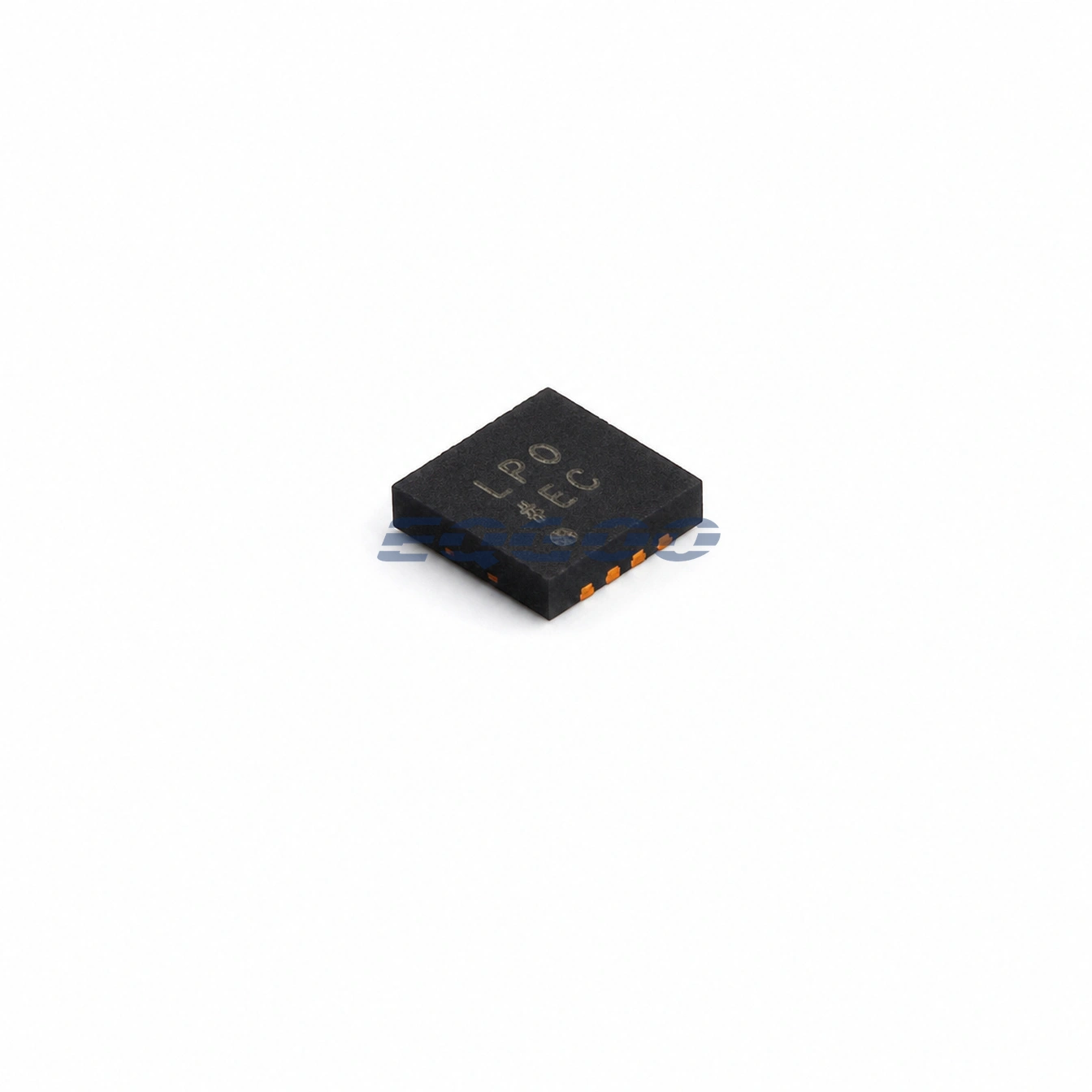
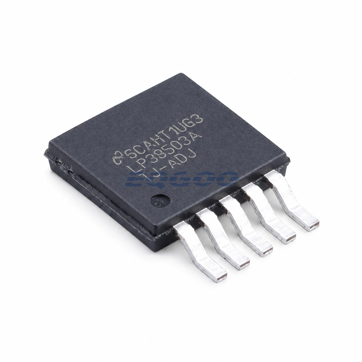
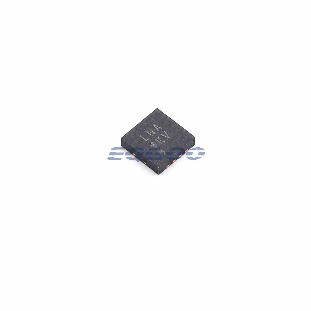
| Package | 8-lead LFCSP_WD, CP-8-11 |
| Operating temperature | −40°C to +125°C |
Product Overview
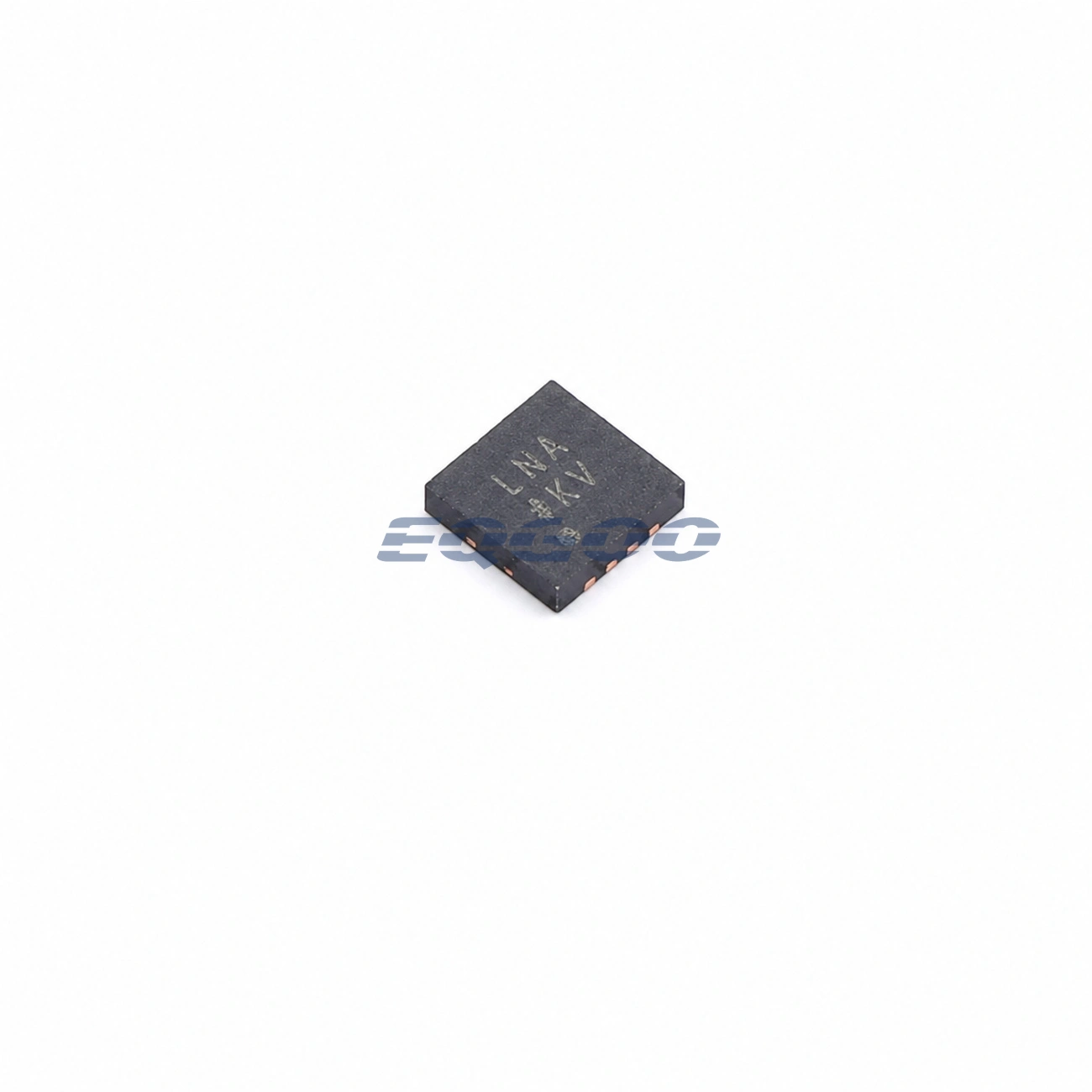
ADM7150ACPZ-3.3-R7 is the fixed 3.3 V LFCSP version of the ADM7150 800 mA low-noise regulator. It accepts 4.5 V to 16 V and targets analog/RF rails where very low integrated noise and strong rejection of upstream ripple are primary selection requirements.
For fixed-output versions, the datasheet specifies 1.0 µV rms integrated noise from 100 Hz to 100 kHz and 1.7 nV/√Hz typical noise density from 10 kHz to 1 MHz. The exact 3.3 V order code avoids an external feedback divider for setting the output voltage.
Key Features
- Fixed 3.3 V output with up to 800 mA load current.
- 4.5 V to 16 V input range.
- 1.0 µV rms integrated noise for fixed-output versions.
- Stable with a 10 µF ceramic output capacitor.
Functional Highlights
The fixed 3.3 V suffix is an electrical characteristic, not only a packaging suffix.
Low-noise results depend on implementation: BYP/REF/VREG capacitors, grounding, capacitor placement, and exposed-pad thermal connection all affect real board performance.
Application Fit
- PLL and VCO supply regulation.
- Noise-sensitive analog and RF circuits.
- Communications infrastructure.
- DAC-driver and instrumentation supply rails.
Design Considerations
- Confirm sufficient input headroom above the fixed 3.3 V output at the required current.
- Calculate power dissipation at the actual VIN and load current.
- Use the recommended 10 µF ceramic output capacitor and reference/bypass components.
- Connect the exposed pad and local ground plane for both thermal and low-noise performance.
Product Status
Manufacturer status: RECOMMENDED FOR NEW DESIGNS
Analog Devices currently marks ADM7150 RECOMMENDED FOR NEW DESIGNS and lists the exact 3.3 V model in its model table.
If the board needs an exposed-pad 8-lead SOIC instead of this 3 mm x 3 mm LFCSP for its fixed 3.3 V analog rail, compare ADM7150ARDZ-3.3-R7. The ADM7150 output setpoint remains 3.3 V and the family supplies up to 800 mA, but the RD-8-2 SOIC and CP-8-11 LFCSP have different PCB footprints, soldering and heat-spreading requirements.
For a low-noise 5.0 V rail rather than this fixed 3.3 V output in the same 8-lead LFCSP ADM7150 package family, review ADM7150ACPZ-5.0-R7. The differing fixed output is a real circuit-level decision: confirm the downstream rail target, regulator input headroom and thermal loading.
Related Engineering Resources
Quality & Verification Support
Third-party inspection or testing can be arranged according to customer requirements. Testing fees are borne by the buyer. Additional verification requirements can be discussed before shipment. After an order is placed, physical product, label, packaging, and Date Code photos may be provided where appropriate.
Request a Quote
To request a quotation, provide the exact manufacturer part number, required quantity, destination, target Date Code if applicable, and any testing or inspection requirements.