
Key Selection Information
| Selection Parameter | Confirmed Information |
|---|---|
| Manufacturer | Alpha & Omega Semiconductor (AOS) |
| Manufacturer Part Number | AO3400A |
| Device Type | N-channel enhancement-mode MOSFET |
| Drain-Source Voltage (VDS) | 30 V maximum |
| Drain Current | 5.7 A at 25 °C in manufacturer parametric data; thermal and PCB conditions must be respected |
| RDS(on), max @ VGS = 10 V | 26.5 mΩ |
| RDS(on), max @ VGS = 4.5 V | 32 mΩ |
| RDS(on), max @ VGS = 2.5 V | 48 mΩ |
| Gate-Source Voltage (VGS) | ±12 V absolute maximum |
| Total Gate Charge | 6 nC typical at VGS = 4.5 V |
| Gate Threshold Voltage | 0.65 V min / 1.05 V typ / 1.45 V max |
| Maximum Junction Temperature | 150 °C |
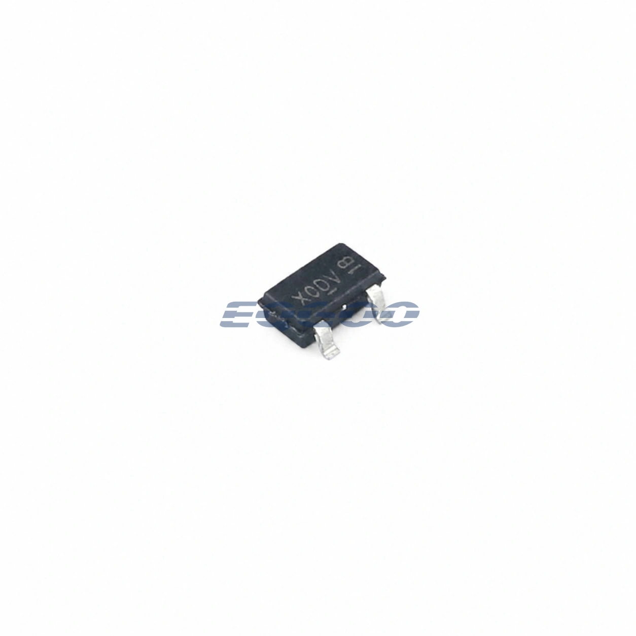
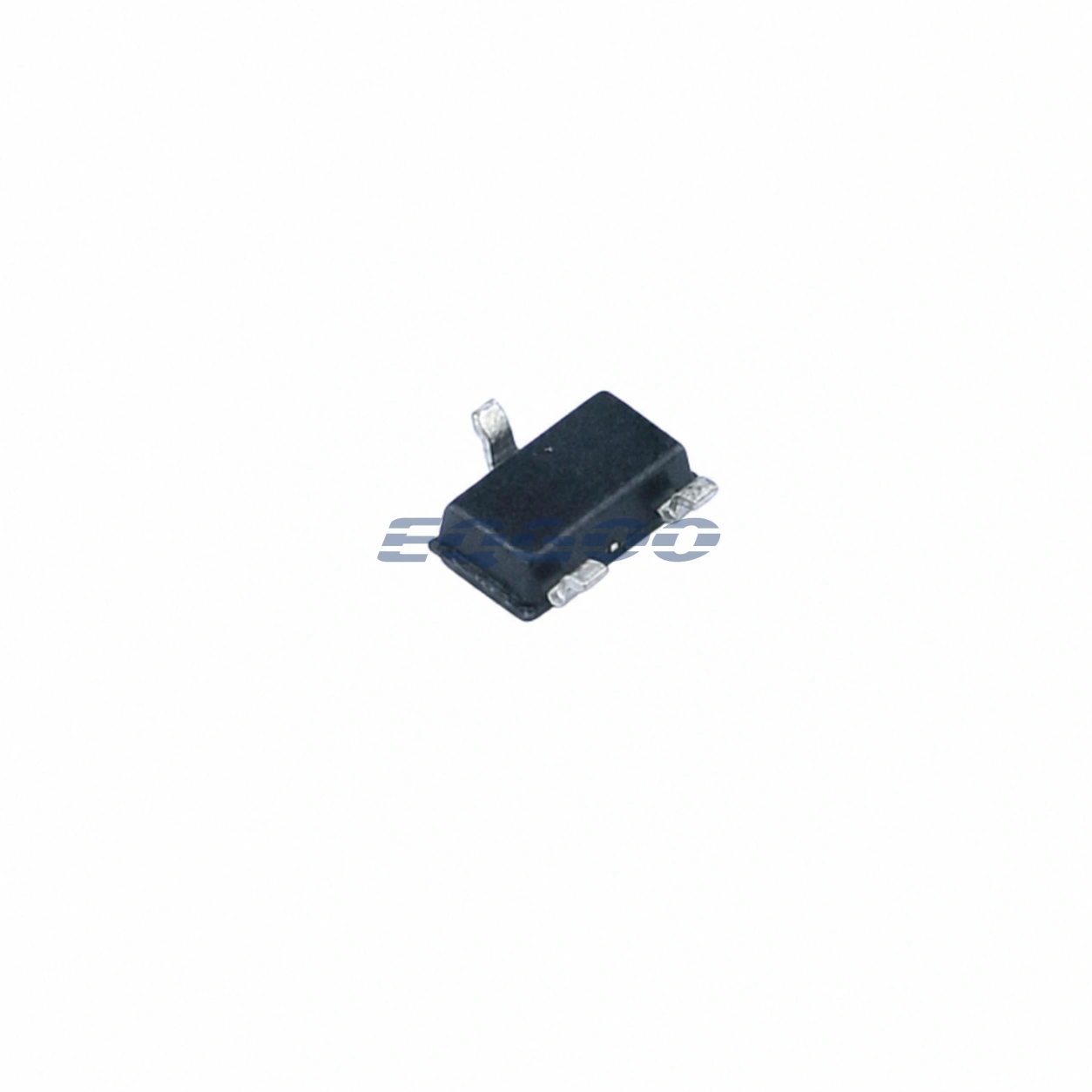
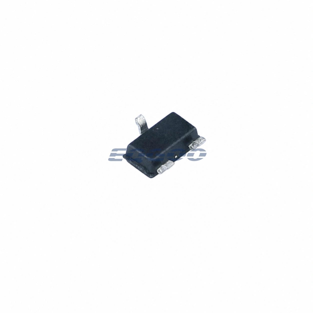
| Package | SOT-23 |
| Manufacturer Status | Full Production |
| Qualification | Industrial |
Product Overview
The AO3400A from Alpha & Omega Semiconductor is a 30 V N-channel MOSFET in a compact SOT-23 package. Its selection profile is defined by low on-resistance across several logic-level gate-drive conditions: AOS specifies a maximum RDS(on) of 26.5 mΩ at VGS = 10 V, 32 mΩ at 4.5 V, and 48 mΩ at 2.5 V. That makes the exact part relevant to low-voltage switching designs where the available gate-drive amplitude may be below 10 V.
AOS lists AO3400A as Full Production and Industrial qualification. The manufacturer describes the device as suitable for load-switching and PWM applications. The 5.7 A drain-current figure shown in manufacturer parametric data is not a stand-alone continuous-current guarantee for every PCB: conduction loss, ambient temperature, copper area, pulse duty cycle, and junction-temperature limits remain part of the real current capability.
Key Features
- 30 V N-channel MOSFET for low-voltage power switching.
- 26.5 mΩ maximum RDS(on) at VGS = 10 V, providing a low conduction-resistance reference at full gate drive.
- 32 mΩ maximum RDS(on) at 4.5 V and 48 mΩ maximum at 2.5 V, useful selection points for logic-level gate-drive systems.
- 5.7 A ID at 25 °C in AOS parametric data; usable continuous current must be checked against actual thermal conditions.
- 6 nC typical total gate charge at VGS = 4.5 V, indicating a relatively modest charge requirement for switching-driver calculations.
- 0.65 V to 1.45 V gate-threshold range, which defines the onset of channel conduction and must not be confused with a recommended full-enhancement gate voltage.
- SOT-23 package with tape-and-reel packaging available from the manufacturer.
- 150 °C maximum junction temperature.
Technical Specifications
| Group | Parameter | Value / Condition |
|---|---|---|
| Device | Polarity | N-channel |
| Device | Configuration | Single |
| Electrical | VDS maximum | 30 V |
| Electrical | VGS absolute maximum | ±12 V |
| Current | ID at 25 °C | 5.7 A, subject to manufacturer thermal / mounting conditions |
| Conduction | RDS(on) max @ VGS = 10 V | 26.5 mΩ |
| Conduction | RDS(on) max @ VGS = 4.5 V | 32 mΩ |
| Conduction | RDS(on) max @ VGS = 2.5 V | 48 mΩ |
| Gate | VGS(th) | 0.65 V min / 1.05 V typ / 1.45 V max |
| Gate | Total Gate Charge Qg @ 4.5 V | 6 nC typical |
| Gate | Gate-Drain Charge Qgd | 1.8 nC |
| Capacitance | Ciss | 630 pF |
| Capacitance | Coss | 75 pF |
| Capacitance | Crss | 50 pF |
| Thermal | Tj maximum | 150 °C |
| Package | Type | SOT-23 |
| Package | Nominal package dimensions | 2.90 × 2.80 mm |
| Qualification | Manufacturer classification | Industrial |
Product Status
| Item | Information |
|---|---|
| Manufacturer Status | Full Production |
Alpha & Omega Semiconductor currently lists AO3400A as a Full Production device on the exact manufacturer product page.
Functional Highlights
Low on-resistance is specified at multiple gate-drive voltages
The 4.5 V and 2.5 V RDS(on) limits are important for logic-driven switching because they provide a defined conduction-resistance reference below the traditional 10 V gate level. This is more useful for selection than relying on gate threshold, which only identifies the beginning of conduction under a small test current.
Gate charge affects switching loss and driver demand
AOS lists 6 nC typical total gate charge at a 4.5 V gate-drive condition. In PWM service, the driver must repeatedly source and remove this charge. Switching frequency, driver impedance, transition time, and the Miller-region charge therefore matter alongside static RDS(on) when estimating total loss.
SOT-23 current capability is thermally constrained
The compact package supports a small PCB footprint, but the same footprint limits heat removal compared with larger power packages. The data-sheet current and power figures must be interpreted with their board and temperature conditions. A low RDS(on) does not eliminate the need to calculate I²R conduction loss and junction-temperature rise.
Applications / Application Fit
- Low-voltage load switching — AOS explicitly identifies load-switching as an application area; the low logic-level RDS(on) values make the device relevant to switched rails and controlled loads within its voltage, current, and thermal envelope.
- PWM-controlled loads — the manufacturer identifies PWM use, and the combination of low on-resistance and modest gate charge can fit PWM switching where gate-drive and thermal calculations are satisfactory.
- Low-side switching from logic-level controllers — 4.5 V and 2.5 V RDS(on) specifications provide useful reference points when a controller or gate driver does not provide a 10 V gate signal.
- Compact motor, fan, solenoid, or LED switching stages — these are engineering-supported categories when the load voltage, transient energy, switching frequency, flyback path, and thermal design remain within the device limits.
Specific automotive qualification, safety certification, or high-reliability application approval should not be inferred from the generic application tags on a product page. AOS classifies the exact part as Industrial.
Why Choose This Part
AO3400A makes technical sense when a 30 V N-channel switch is needed in SOT-23 and the available gate-drive voltage is in the 2.5 V to 4.5 V logic range. Because AOS publishes maximum RDS(on) values at both 4.5 V and 2.5 V, the designer can estimate conduction loss without assuming that the MOSFET will be driven at 10 V.
A different MOSFET may be more appropriate when the design requires substantially higher drain voltage, a larger continuous thermal margin, avalanche requirements beyond the exact datasheet conditions, or a power package with lower thermal resistance.
Design Considerations
Do not use VGS(th) as the gate-drive target. The 0.65 V to 1.45 V threshold range indicates when the channel begins to conduct under the datasheet test condition; it does not mean the MOSFET reaches the listed low RDS(on) at that gate voltage. Use the RDS(on) condition closest to the real gate-drive level.
Preserve thermal conditions around current ratings. The 5.7 A parametric value is tied to 25 °C manufacturer conditions. Estimate conduction and switching loss, then verify junction temperature using the actual PCB copper, ambient temperature, airflow, duty cycle, and manufacturer thermal data.
Allow voltage margin above normal load voltage. The 30 V VDS figure is an absolute device limit, not a recommended operating target. Inductive loads, cable inductance, and switching loops can generate overshoot; snubbing or clamping may be required so transients remain within the MOSFET rating.
Gate-drive loss increases with switching frequency. The 6 nC typical gate-charge figure is useful for estimating average gate-drive demand, while Qgd and driver impedance influence transition time. At higher PWM frequencies, switching loss can become significant even when conduction loss is modest.
Inductive loads require an energy path. A motor, relay, solenoid, or other inductive load can force current to continue when the MOSFET turns off. The system must provide a suitable freewheel, clamp, or other transient-control path appropriate to the topology.
Related Engineering Resources
- AOS AO3400A product page — official manufacturer page with status, parametric values, documentation, package details, and qualification.
- AOS AO3400A datasheet — manufacturer datasheet for detailed electrical, switching, thermal, and test-condition information.
FAQ
What is the maximum drain-source voltage of AO3400A?
The maximum VDS rating is 30 V. Normal operating voltage should include margin for switching and inductive transients rather than treating 30 V as a recommended working point.
Can AO3400A be driven from 3.3 V logic?
AOS specifies maximum RDS(on) at VGS = 2.5 V and 4.5 V, so the device has characterized low-resistance operation in the logic-level range. The exact loss at a 3.3 V gate level should still be evaluated using the datasheet curves and the application’s current and temperature conditions.
Is the 1 V-class gate threshold a suitable ON-state drive voltage?
No. Gate threshold describes the onset of conduction at a small test current. Low-resistance switching requires a higher gate voltage; use the manufacturer’s RDS(on) conditions as the selection reference.
What RDS(on) does AOS specify?
AOS lists 26.5 mΩ maximum at VGS = 10 V, 32 mΩ maximum at 4.5 V, and 48 mΩ maximum at 2.5 V. The datasheet conditions associated with those limits should be preserved in loss calculations.
Is AO3400A an automotive-qualified MOSFET?
The official AO3400A product page classifies the part as Industrial. Do not infer AEC-Q100/AEC-Q101 qualification from a generic automotive application tag; qualification for a regulated design must be verified from manufacturer documentation for the exact ordering code.
Alternative Candidates for Engineering Evaluation
| MPN | Manufacturer | Package |
|---|---|---|
| FH3400B | 鑫飞宏 | SOT-23 |
| AO3400 | HKT (合科泰) | SOT-23 |
| AO3400A | baocheng (宝乘) | SOT-23 |
| FH3400BL | 鑫飞宏 | SOT-23-3L |
| AO3400 | TECH PUBLIC (台舟) | SOT-23-3L |
Candidate alternative parts require engineering verification before substitution. Electrical characteristics, pinout, package, qualification, and application requirements should be verified before use.
Quality & Verification Support
Third-party inspection or testing can be arranged according to customer requirements. Testing fees are borne by the buyer. Additional verification requirements can be discussed before shipment. After an order is placed, physical product, label, packaging, and Date Code photos may be provided where appropriate.
Request a Quote
To request a quotation, provide the manufacturer part number, required quantity, destination, target Date Code if applicable, and any testing or inspection requirements.