
Key Selection Information
| Selection Parameter | Confirmed Information |
|---|---|
| Manufacturer | STMicroelectronics |
| Manufacturer Part Number | STM32F103C8T6 |
| Manufacturer Status | Active / volume production |
| Core | 32-bit Arm Cortex-M3 |
| Maximum CPU Frequency | 72 MHz |
| Flash Memory | 64 KB |
| SRAM | 20 KB |
| Supply Voltage | 2.0 V to 3.6 V |
| ADC | 2 × 12-bit, 1 µs conversion |
| Communication | Up to 2 × I²C, 2 × SPI, 3 × USART, USB 2.0 FS, CAN 2.0B Active |
| Timers | 3 general-purpose 16-bit timers + 1 advanced motor-control PWM timer, plus watchdogs and SysTick |
| DMA | 7 channels |
| GPIO on LQFP-48 | 37 I/Os |
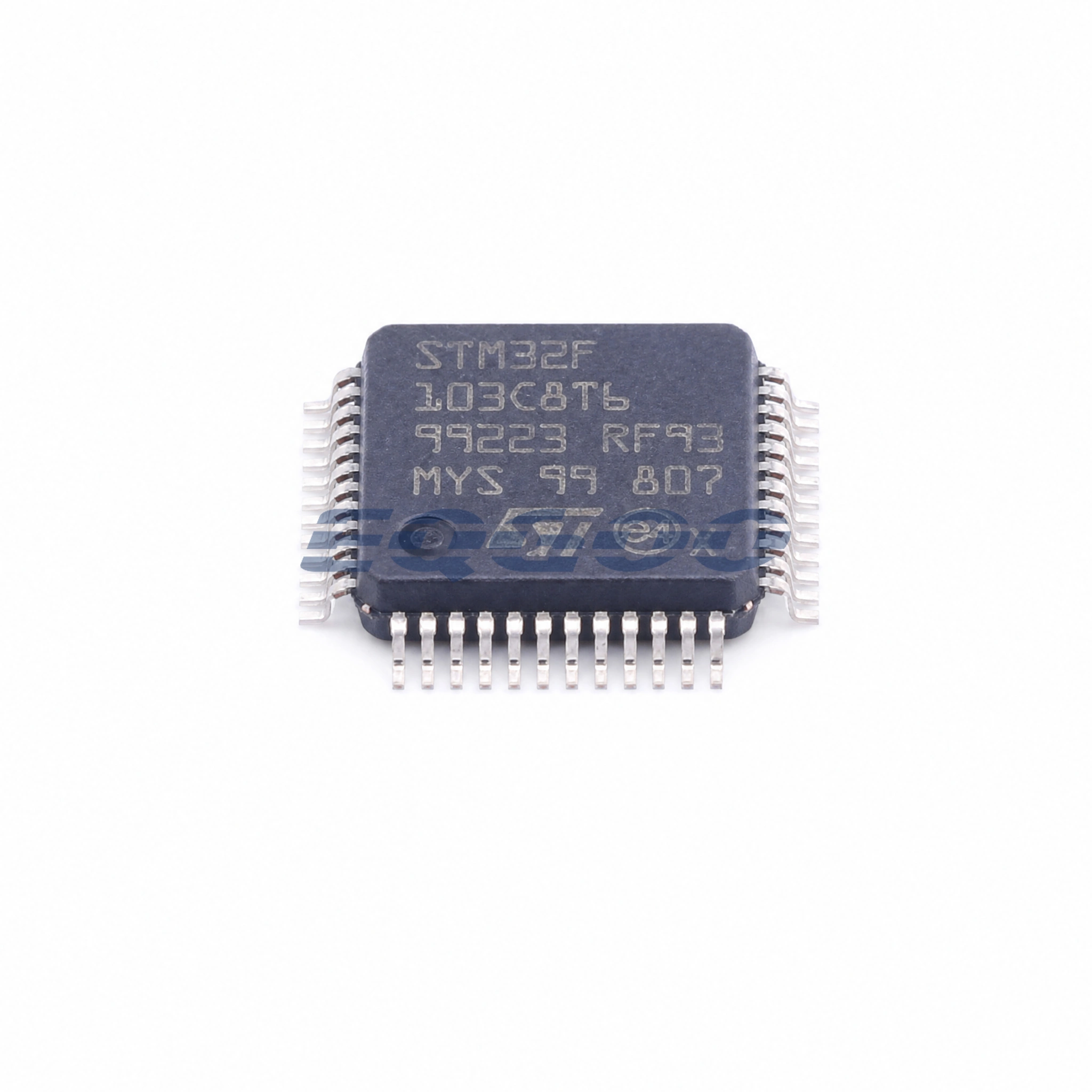
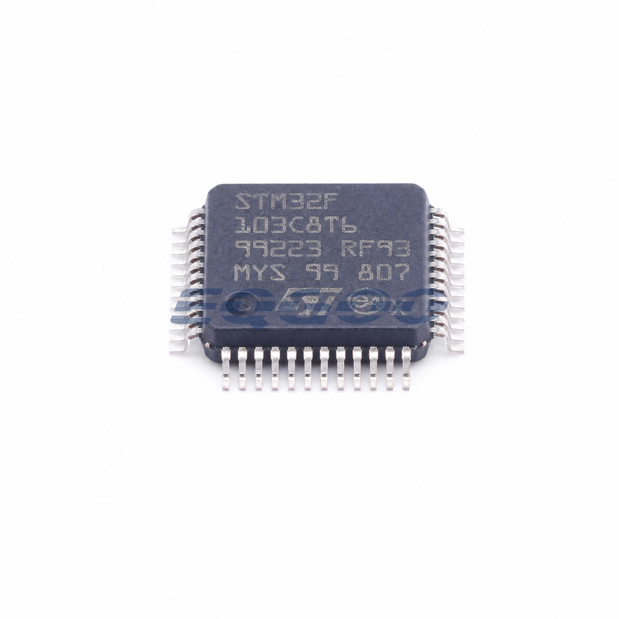
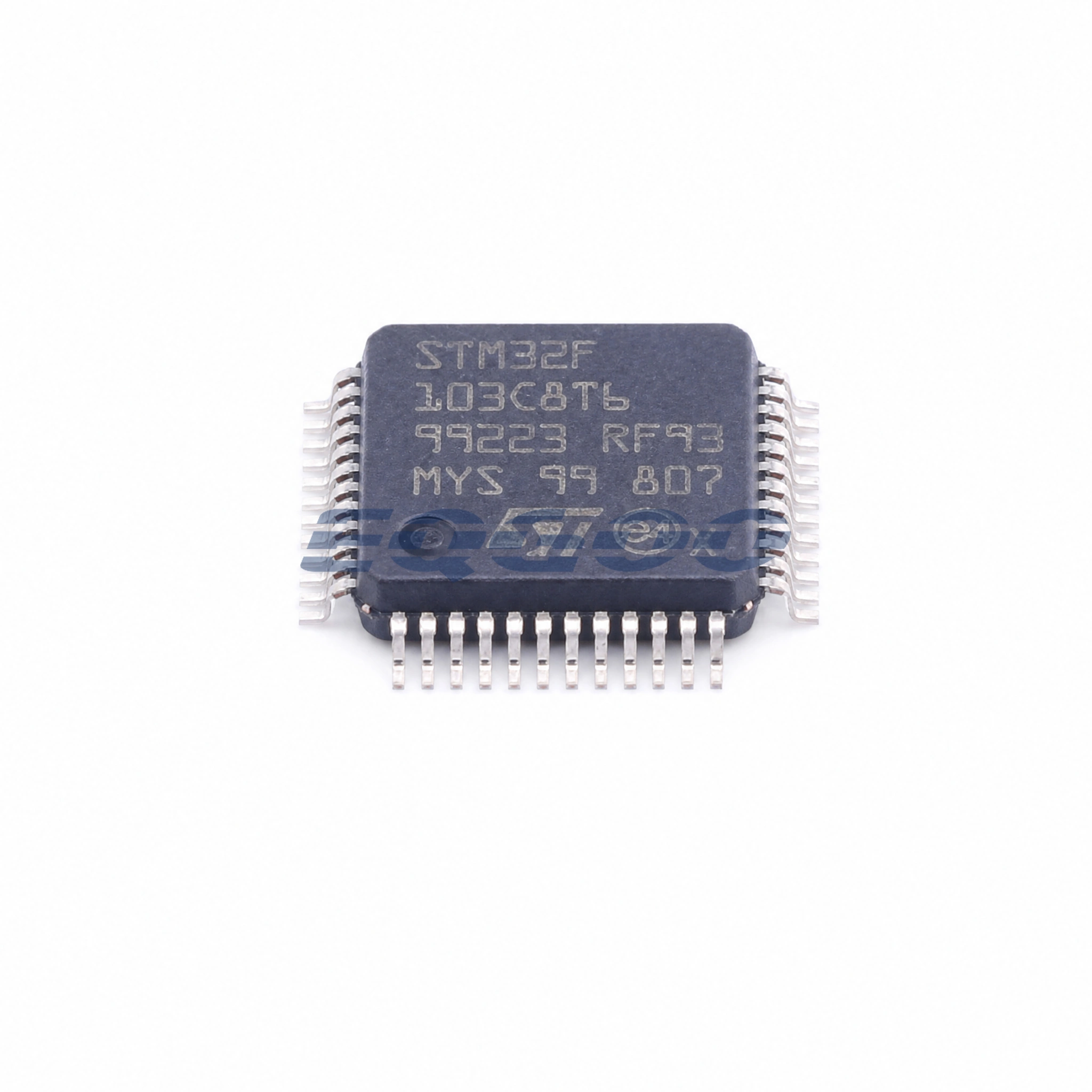
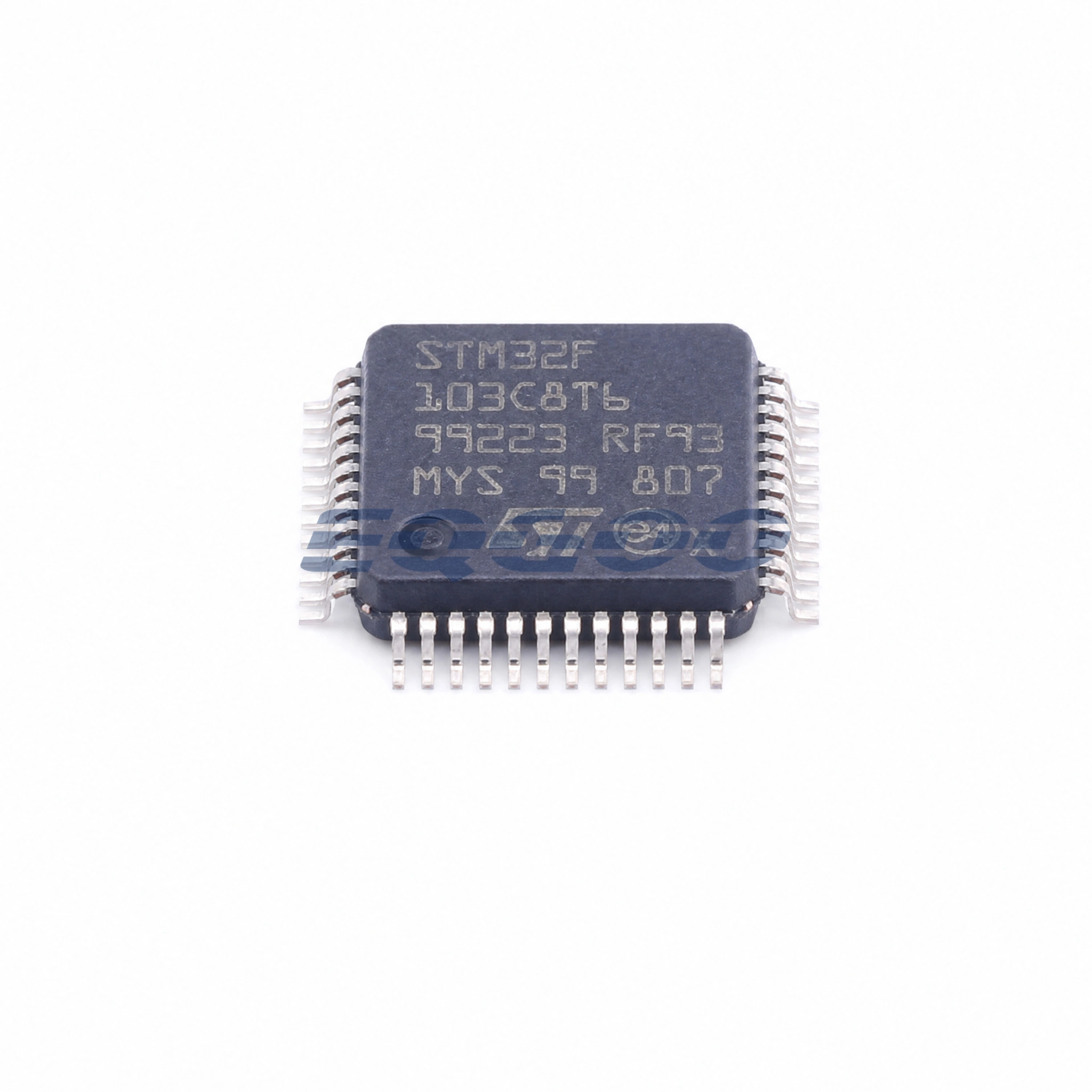
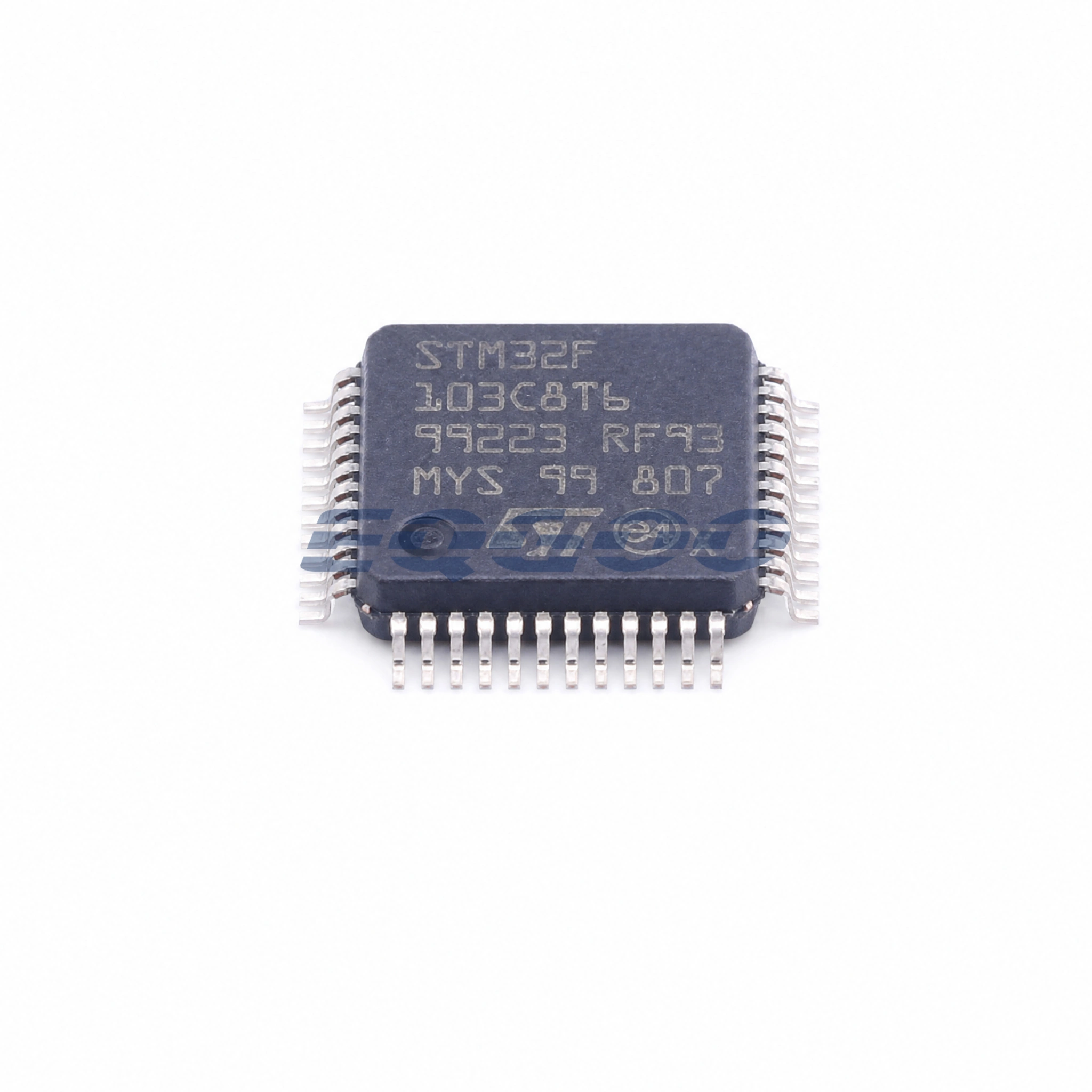
| Package | LQFP-48, 7 × 7 × 1.4 mm |
| Operating Temperature | -40 °C to +85 °C for T6 grade |
| Qualification | Industrial, Ecopack2 |
Product Overview
The STM32F103C8T6 is a medium-density STM32F1 microcontroller built around a 72 MHz Arm Cortex-M3 core. The exact C8T6 ordering code combines 64 KB of embedded Flash, 20 KB of SRAM, a 48-pin LQFP package, industrial -40 °C to +85 °C temperature grade, and a 2.0 V to 3.6 V operating supply.
The device integrates two 12-bit ADCs, a 7-channel DMA controller, three general-purpose 16-bit timers, an advanced motor-control PWM timer, watchdog timers, USB 2.0 full-speed, CAN 2.0B Active, and multiple I²C, SPI, and USART interfaces. This peripheral mix makes it relevant to embedded-control designs that need moderate processing capability together with analog acquisition and several communication interfaces.
Key Features
- 32-bit Arm Cortex-M3 core running at up to 72 MHz.
- 64 KB embedded Flash and 20 KB SRAM.
- 2.0 V to 3.6 V supply range.
- Two 12-bit ADCs with 1 µs conversion time.
- Up to two I²C interfaces, two SPI interfaces, and three USARTs.
- USB 2.0 full-speed device interface.
- CAN 2.0B Active controller.
- 16-bit advanced motor-control PWM timer with dead-time generation and emergency-stop capability.
- Seven-channel DMA controller.
- SWD and JTAG debug support.
- LQFP-48 package with 37 I/Os.
- Sleep, Stop, and Standby low-power modes with VBAT support for RTC / backup domain.
Technical Specifications
| Group | Parameter | Value |
|---|---|---|
| Core | Architecture | Arm Cortex-M3, 32-bit |
| Core | Maximum frequency | 72 MHz |
| Memory | Flash | 64 KB |
| Memory | SRAM | 20 KB |
| Supply | VDD | 2.0 V to 3.6 V |
| Analog | ADC | 2 × 12-bit, 1 µs |
| Analog | Conversion range | 0 V to 3.6 V |
| Communication | I²C | Up to 2 |
| Communication | SPI | Up to 2, up to 18 Mbit/s |
| Communication | USART | Up to 3 |
| Communication | CAN | CAN 2.0B Active |
| Communication | USB | USB 2.0 full-speed |
| DMA | Channels | 7 |
| Timers | General-purpose | 3 × 16-bit |
| Timers | Advanced-control | 1 × 16-bit motor-control PWM timer |
| Debug | Interfaces | SWD, JTAG |
| Security / ID | Unique device ID | 96-bit |
| Package | Type | LQFP-48 |
| Package | Body size | 7 × 7 × 1.4 mm |
| GPIO | I/O count on LQFP-48 | 37 |
| Operating | Temperature | -40 °C to +85 °C |
Product Status
| Item | Information |
|---|---|
| Manufacturer Status | Active / volume production |
STMicroelectronics currently lists STM32F103C8 as Active and the exact STM32F103C8T6 orderable code as an industrial-grade production part.
Functional Highlights
72 MHz Cortex-M3 with 64 KB Flash defines the performance tier
The C8T6 combines a 72 MHz Cortex-M3 core with 64 KB of Flash and 20 KB of SRAM. The Flash capacity is an important exact-variant boundary: firmware size, protocol stacks, bootloader space, and future feature growth should be checked against the 64 KB limit before the part is frozen into a design.
Integrated USB and CAN reduce external protocol-controller requirements
The MCU includes both a USB 2.0 full-speed device interface and a CAN 2.0B Active controller. These blocks provide the protocol-controller functions on chip; CAN still requires an external physical-layer transceiver, and USB still requires the appropriate connector, routing, clocking, ESD, and power implementation.
Advanced timer and ADC resources support control-oriented designs
The advanced 16-bit PWM timer includes dead-time generation and emergency-stop support, while the dual 12-bit ADCs provide analog acquisition. Together with DMA, these peripherals can support control loops, PWM generation, and sampled feedback when the application’s timing and analog requirements fit the documented capabilities.
Multiple serial interfaces allow mixed-peripheral systems
With up to three USARTs, two I²C buses, and two SPI interfaces, the device can connect to several external digital peripherals without forcing all traffic onto a single bus. Exact pin multiplexing must still be checked for the LQFP-48 package because not every peripheral signal can be used simultaneously on every pin assignment.
Applications / Application Fit
STM32F103C8T6 can be considered for embedded-control designs that need a 32-bit MCU with moderate code space, analog acquisition, timers, and several communication interfaces.
Engineering-supported application categories include:
- motor-control logic using the advanced PWM timer, ADCs, and DMA;
- USB-connected embedded peripherals;
- CAN-based communication nodes when paired with an external CAN transceiver;
- sensor acquisition and local control systems using ADC, timers, and serial buses;
- general embedded controllers that need multiple UART, SPI, or I²C links.
Formal automotive, medical, safety, or other regulated qualification must not be inferred from the general peripheral set. The exact STM32F103C8T6 ordering code is listed by ST as Industrial grade.
Why Choose This Part
STM32F103C8T6 makes technical sense when a design needs the STM32F1 Cortex-M3 architecture, up to 72 MHz CPU speed, 64 KB of Flash, 20 KB of SRAM, USB, CAN, dual ADCs, and motor-control-capable timing in a 48-pin LQFP package.
A different family member should be considered when the firmware needs more than 64 KB of Flash, when a different package or I/O count is required, when the temperature grade must exceed +85 °C, or when newer security, low-power, or peripheral features are a primary design requirement.
Design Considerations
Flash headroom: The exact C8T6 has 64 KB of Flash. Check final linked firmware size, bootloader requirements, middleware, and future update margin rather than relying only on an early prototype build.
CAN physical layer: The on-chip CAN block is the protocol controller. An external CAN transceiver is required between the MCU pins and the differential bus.
USB implementation: The USB full-speed controller does not eliminate board-level USB design requirements. Verify the required clock configuration, connector, ESD protection, power architecture, and differential routing.
ADC pin availability: The family supports up to 16 ADC channels, but the LQFP-48 package exposes a smaller subset. Confirm the exact pinout and alternate-function mapping before assigning analog channels.
GPIO voltage tolerance: ST states that almost all I/Os are 5 V tolerant, but this applies only to the pins identified accordingly in the datasheet and does not change the 2.0 V to 3.6 V MCU supply requirement.
Pin multiplexing: USB, CAN, timers, debug, and serial interfaces share alternate-function resources. Check the exact LQFP-48 pin map early so required functions do not collide.
Temperature grade: T6 is the -40 °C to +85 °C industrial-temperature code. Designs requiring the extended +105 °C grade need the appropriate exact ordering code.
Related Engineering Resources
- STMicroelectronics STM32F103C8 product page — official status, device overview, features, and quality information.
- STM32F103x8/xB datasheet — official electrical, pinout, package, and device-family specification.
- STM32F1 documentation page — official datasheets, reference manual RM0008, programming manuals, and errata.
FAQ
How much Flash does STM32F103C8T6 have?
The exact C8T6 ordering code has 64 KB of embedded Flash.
How much SRAM is available?
The medium-density STM32F103C8 device provides 20 KB of SRAM.
Does the MCU include USB and CAN?
Yes. It includes USB 2.0 full-speed and a CAN 2.0B Active controller. CAN still requires an external transceiver for the physical bus.
What package does STM32F103C8T6 use?
The exact T6 orderable code uses a 48-pin LQFP package with a 7 × 7 × 1.4 mm body.
What temperature range applies to T6?
The T6 grade is specified for -40 °C to +85 °C operation.
How many GPIOs are available in the LQFP-48 package?
ST lists 37 I/Os for the LQFP-48 / 48-pin device configuration. Actual usable pins depend on the selected alternate functions, oscillator, debug, analog, and communication assignments.
Quality & Verification Support
Third-party inspection or testing can be arranged according to customer requirements. Testing fees are borne by the buyer. Additional verification requirements can be discussed before shipment. After an order is placed, physical product, label, packaging, and Date Code photos may be provided where appropriate.
Request a Quote
To request a quotation, provide the manufacturer part number, required quantity, destination, target Date Code if applicable, and any testing or inspection requirements.