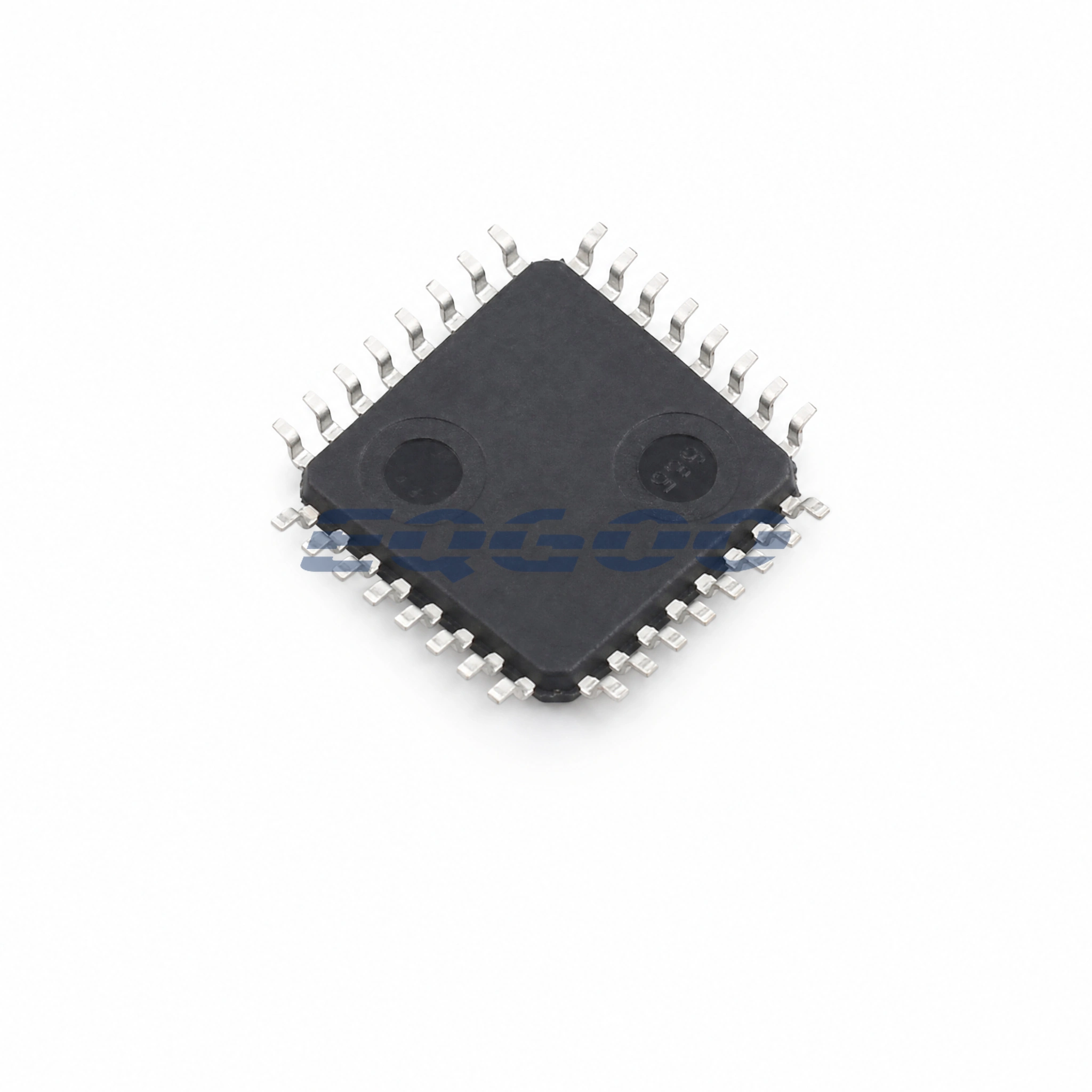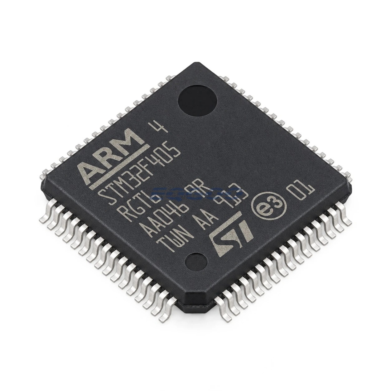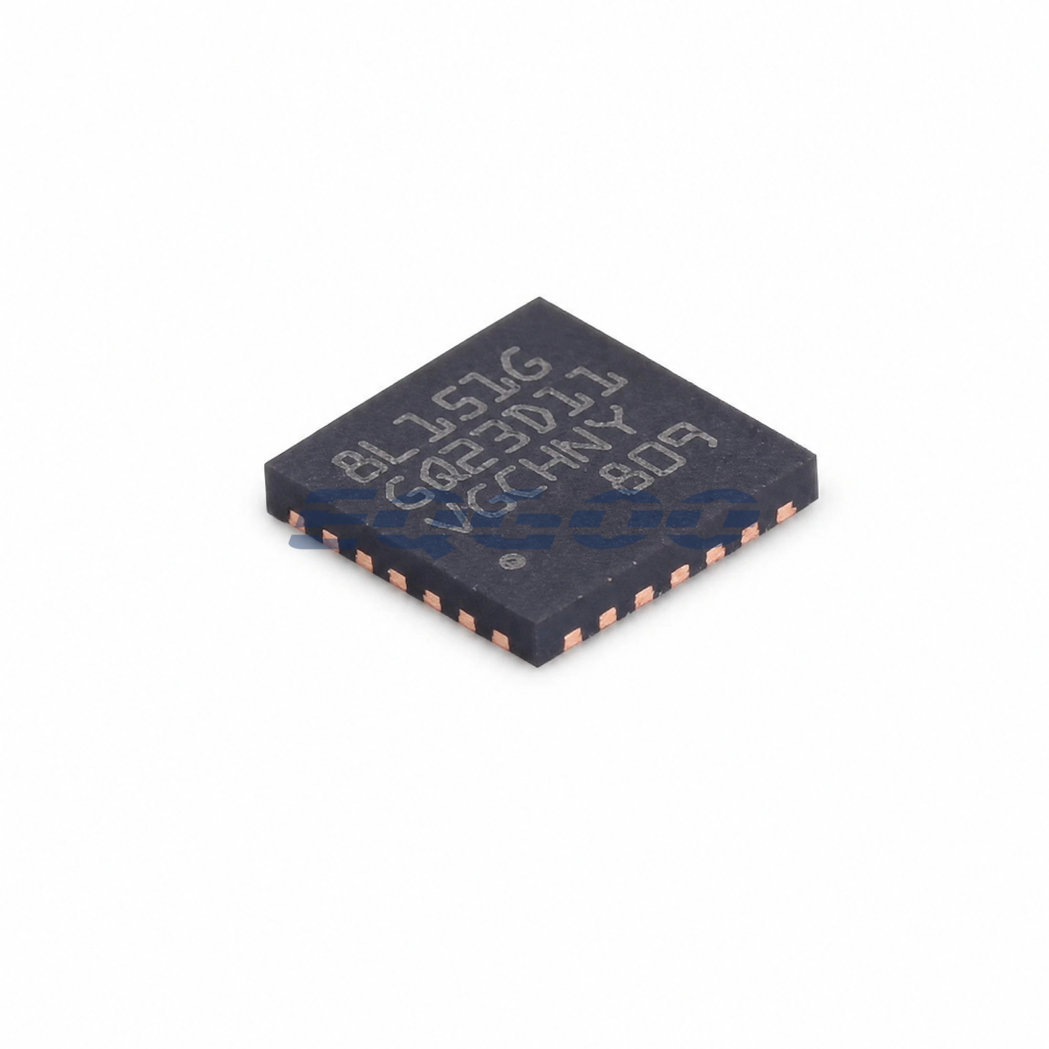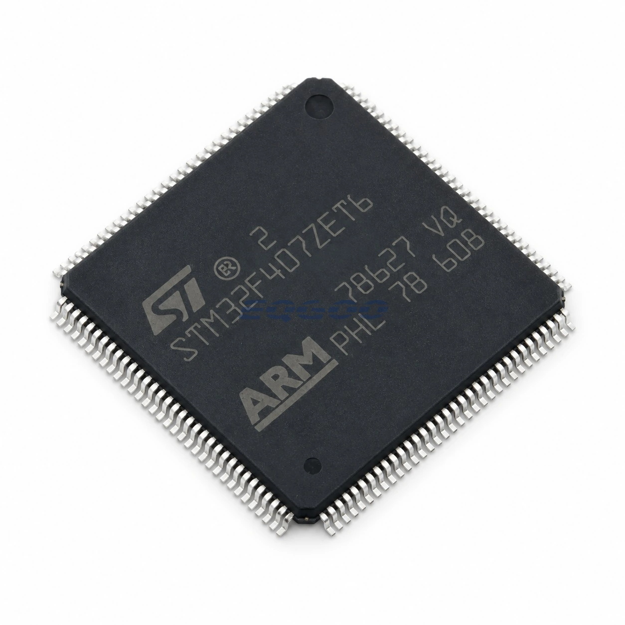
Key Selection Information
| Selection Parameter | Confirmed Information |
|---|---|
| Package | LQFP-144(20×20) |
| Supply voltage | 1.8V~3.6V |
| CPU Core | ARM Cortex-M4 |
| Maximum CPU speed | 168MHz |
| Program memory | 512KB |
| Operating Temperature | -40℃~+85℃ |
| Number of I/O | 114 |
512 KB F407 with 144-pin I/O headroom
STM32F407ZET6 keeps the 168 MHz Cortex-M4, FPU/DSP and 512 KB Flash profile of the F407E density but moves it into LQFP-144. ST lists 114 I/Os for the exact ZET6 orderable, substantially more than the 82 I/Os on the 100-pin VET6.
The device includes the F407 connectivity set: 10/100 Ethernet MAC with IEEE 1588 support, parallel camera interface, USB OTG, two CAN controllers, three ADCs and two DACs. The Z package is therefore primarily about exposing more of that peripheral set to the board.
Technical Specifications
| Parameter | Value |
|---|---|
| Package | LQFP-144(20×20) |
| Supply voltage | 1.8V~3.6V |
| CPU Core | ARM Cortex-M4 |
| Maximum CPU speed | 168MHz |
| Program memory | 512KB |
| Operating Temperature | -40℃~+85℃ |
| Number of I/O | 114 |
| DAC (Bit) | 12bit |
| ADC (Bit) | 12bit |
| Program Memory Type | FLASH |
| Core Size | 32 Bit |
| Oscillator Type | Built-in |
Choose ZE for pins, not for extra Flash
ZET6 still has 512 KB of Flash. Its advantage over VET6 is the LQFP-144 package and 114-I/O budget, not a larger memory density. If the board needs the same 144-pin package but 1 MB of Flash, ZGT6 is the closer step up.
Use the extra pins deliberately
The larger package makes combinations such as Ethernet, camera, external memory and multiple serial buses easier to route without exhausting GPIO as quickly as LQFP-100. That does not remove alternate-function conflicts; it simply gives the designer a wider package-level signal budget.
When ZET6 is preferable
This orderable is a good fit when F407 connectivity is required and the design is pin-limited rather than memory-limited. It is especially relevant when several high-pin-count interfaces must coexist but 512 KB of program Flash remains sufficient.
Separate interface silicon from MCU capability
Ethernet still requires an external PHY, and USB high-speed designs require the external ULPI PHY path. The 144-pin package also increases routing density and power-distribution complexity, so the extra I/O count should be matched to a concrete interface plan rather than treated as free expansion.
For increased program Flash within the STM32F407 LQFP-144 family, compare STM32F407ZGT6 (1 MB Flash) with this ZET6 variant (512 KB). Both use 144-pin LQFP order codes, but confirm memory map, board pinout and firmware requirements before altering a qualified BOM.
Related Engineering Resources
- STM32F407ZET6 Datasheet (PDF) — HKEQGOO-hosted copy of the STMicroelectronics datasheet used for technical review.
- STMicroelectronics product page — official manufacturer product, lifecycle, ordering and documentation resource.
Quality & Verification Support
Third-party inspection or testing can be arranged according to customer requirements. Testing fees are borne by the buyer. Additional verification requirements can be discussed before shipment. After an order is placed, physical product, label, packaging, and Date Code photos may be provided where appropriate.
For 512 KB Flash in a smaller 100-pin LQFP rather than this 144-pin package, review STM32F407VET6. Both are STM32F407E-density devices, but fewer available I/Os and a different footprint can affect the peripheral breakout, routing and PCB redesign.
Request a Quote
To request a quotation, provide the manufacturer part number, required quantity, destination, target Date Code if applicable, and any testing or inspection requirements.