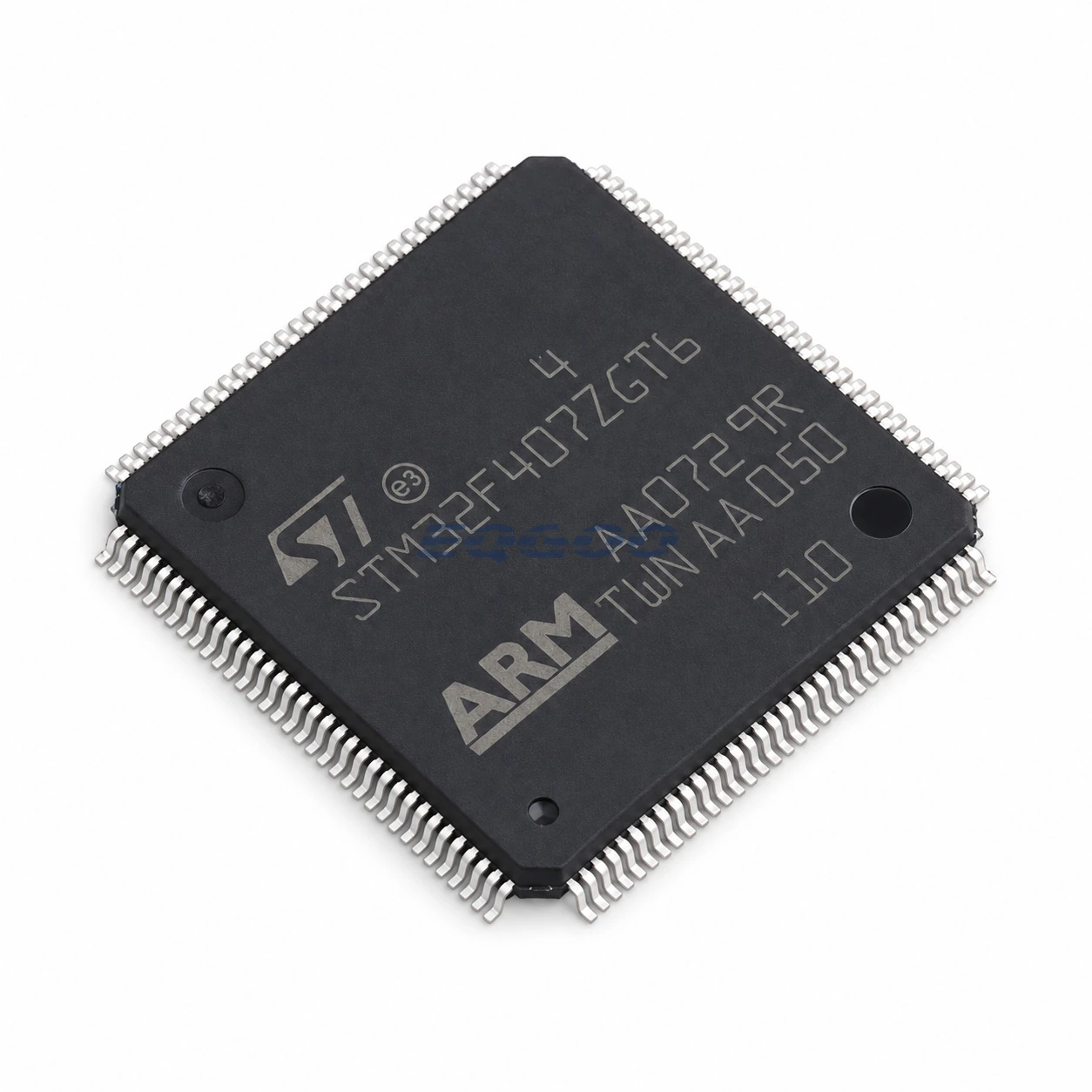
Key Selection Information
| Selection Parameter | Confirmed Information |
|---|---|
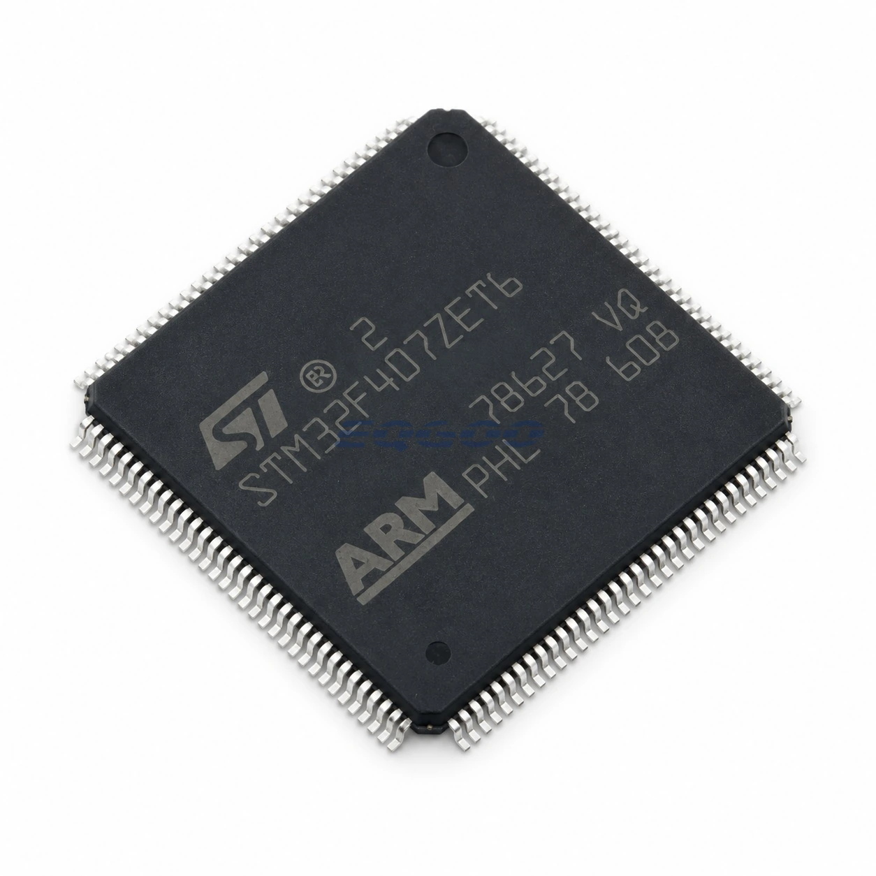
| Package | LQFP-144(20×20) |
| Supply voltage | 1.8V~3.6V |
| CPU Core | ARM Cortex-M4 |
| Maximum CPU speed | 168MHz |
| Program memory | 1MB |
| Operating Temperature | -40℃~+85℃ |
| Number of I/O | 114 |
1 MB F407 in LQFP-144
STM32F407ZGT6 combines the largest 1 MB Flash option in this F407 group with the 144-pin LQFP package. The device runs a 168 MHz Cortex-M4 core with FPU/DSP support, and ST lists 114 I/Os for the exact ZGT6 orderable.
The F407 connectivity block includes 10/100 Ethernet MAC, a parallel camera interface, USB OTG and two CAN controllers alongside the F4 analog, timer and DMA resources. For this part, the key selection combination is therefore 1 MB Flash plus 114 package I/Os.
Technical Specifications
| Parameter | Value |
|---|---|
| Package | LQFP-144(20×20) |
| Supply voltage | 1.8V~3.6V |
| CPU Core | ARM Cortex-M4 |
| Maximum CPU speed | 168MHz |
| Program memory | 1MB |
| Operating Temperature | -40℃~+85℃ |
| Number of I/O | 114 |
| DAC (Bit) | 12bit |
| ADC (Bit) | 12bit |
| Program Memory Type | FLASH |
| Core Size | 32 Bit |
| Oscillator Type | Built-in |
The difference from ZET6 is memory density
ZGT6 and ZET6 share the same LQFP-144 package class and 114-I/O count, but ZGT6 raises program Flash from 512 KB to 1 MB. That makes ZGT6 the stronger choice when the PCB already needs the 144-pin F407 footprint and firmware size, networking stacks or future feature growth would make 512 KB restrictive.
Memory headroom and interface concurrency
One megabyte of Flash solves code-space pressure, not pin-multiplexing conflicts. Ethernet, camera, external memory, USB, CAN and serial buses still need to be mapped against the exact alternate-function table. The 144-pin package gives more freedom, but interface concurrency should be proven before layout.
Best use of the ZGT6 configuration
This orderable is most compelling for feature-rich connected controllers where both a large I/O budget and 1 MB of program storage matter. If the design needs the same connectivity but only 512 KB of Flash, ZET6 can meet the package requirement without paying for unused memory capacity.
System-level implementation
Plan external Ethernet PHY, USB HS ULPI PHY where high-speed USB is required, CAN transceivers, memory-bus loading and camera routing as board-level resources. The MCU integrates the controllers, but not every external physical layer. At 168 MHz and with a dense 144-pin interface map, clock, decoupling and return-path planning remain part of the component-selection decision.
For an STM32F407 LQFP-144 configuration with 512 KB Flash instead of this 1 MB ZGT6 orderable, compare STM32F407ZET6. Confirm application image size and Flash sector use, as well as the exact order-code and pin requirements, before changing the BOM.
Related Engineering Resources
- STM32F407ZGT6 Datasheet (PDF) — HKEQGOO-hosted copy of the STMicroelectronics datasheet used for technical review.
- STMicroelectronics product page — official manufacturer product, lifecycle, ordering and documentation resource.
Quality & Verification Support
Third-party inspection or testing can be arranged according to customer requirements. Testing fees are borne by the buyer. Additional verification requirements can be discussed before shipment. After an order is placed, physical product, label, packaging, and Date Code photos may be provided where appropriate.
When 1 MB of program Flash is needed but the board uses a smaller 100-pin LQFP footprint instead of this 144-pin package, compare STM32F407VGT6. The STM32F407 core family and flash density are shared; fewer exposed I/O pins, pin mapping and the 14 x 14 mm board outline require a separate schematic and PCB review.
Request a Quote
To request a quotation, provide the manufacturer part number, required quantity, destination, target Date Code if applicable, and any testing or inspection requirements.