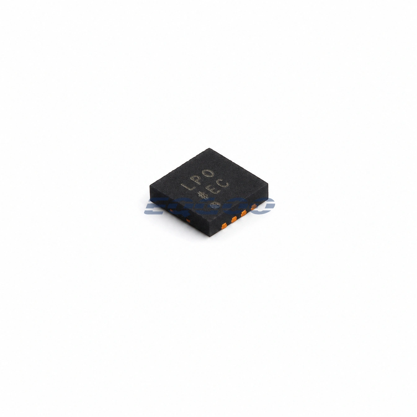
Key Selection Information
| Selection Parameter | Confirmed Information |
|---|---|
| Input voltage | 2.3 V to 6.5 V |
| Fixed output | 3.3 V |
| Maximum load current | 2 A |
| Output noise | 5 µV rms, 100 Hz to 100 kHz |
| PSRR | 60 dB at 100 kHz |
| Dropout | 172 mV at 2 A, VOUT = 3 V family condition |
| Accuracy | ±1.5% over line, load, and temperature |
| Output capacitor | Stable with 4.7 µF ceramic |
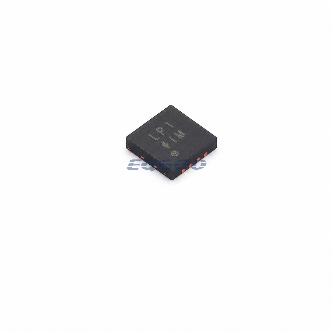
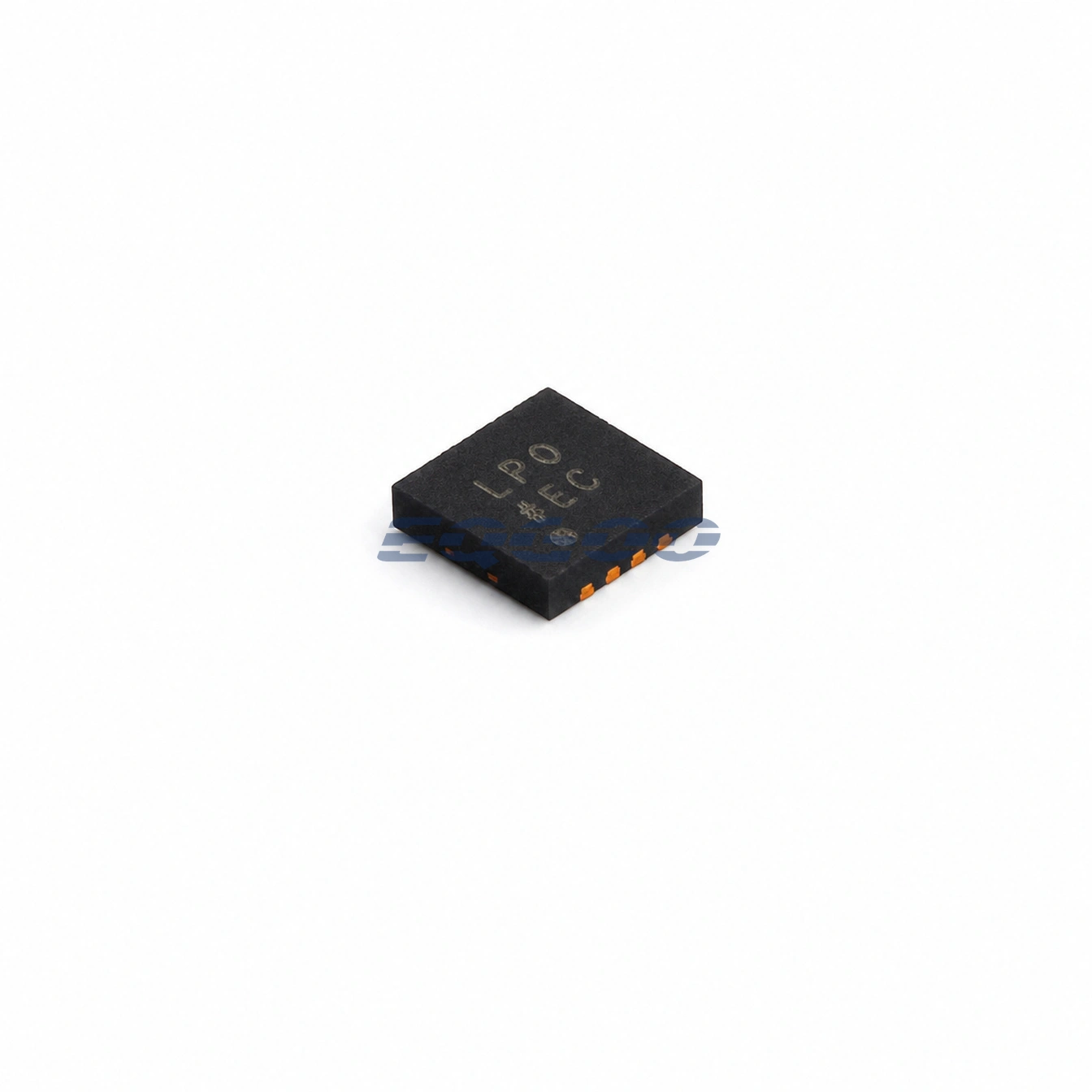
| Package | 8-lead 3 mm × 3 mm LFCSP, CP-8-21 |
| Operating temperature | −40°C to +125°C |
Product Overview
ADM7172ACPZ-3.3-R7 is the fixed 3.3 V version of the ADM7172 2 A low-noise CMOS LDO. Although the family accepts inputs down to 2.3 V, a 3.3 V output requires VIN to stay above 3.3 V by enough headroom for regulation at the intended load.
The fixed-output order code provides the family low-noise and high-PSRR architecture without an external feedback divider. It is suited to high-current 3.3 V analog rails where supply cleanliness matters more than conversion efficiency alone.
Key Features
- Fixed 3.3 V output with up to 2 A load current.
- 5 µV rms output noise.
- 60 dB PSRR at 100 kHz.
- Stable with a 4.7 µF ceramic output capacitor.
Functional Highlights
The -3.3-R7 suffix fixes the output voltage; the related ACPZ-R7 part without the voltage suffix is adjustable.
At high current, LDO loss becomes heat. The voltage dropped from VIN to 3.3 V, multiplied by load current, sets the main thermal burden.
Application Fit
- 3.3 V supplies for ADC and DAC circuits.
- Precision amplifier and clocking rails.
- PLL/VCO and mixed-signal supply filtering.
- Instrumentation and communications circuitry.
Design Considerations
- Do not use the adjustable-version feedback divider; this model is internally fixed at 3.3 V.
- Verify VIN headroom above 3.3 V across load, line, and temperature.
- Calculate thermal dissipation and use the exposed pad/PCB copper appropriately.
- Meet the 4.7 µF output-capacitor requirements and keep sensitive nodes away from switching noise.
Product Status
Manufacturer status: RECOMMENDED FOR NEW DESIGNS
Analog Devices currently marks the ADM7172 family RECOMMENDED FOR NEW DESIGNS.
If a programmable output is needed instead of the internally fixed 3.3 V rail on this part, review ADM7172ACPZ-R7. The adjustable ADM7172 version requires an external feedback divider to establish the output voltage; check the feedback network, rail target and dropout margin before redesign.
For a fixed 5.0 V rail instead of this fixed 3.3 V ADM7172 output, compare ADM7172ACPZ-5.0-R7. Both are 2 A ADM7172-family LFCSP orderables, but the programmed output voltage changes the required input headroom and regulator thermal dissipation; do not substitute one without checking the actual rail requirement.
Related Engineering Resources
Quality & Verification Support
Third-party inspection or testing can be arranged according to customer requirements. Testing fees are borne by the buyer. Additional verification requirements can be discussed before shipment. After an order is placed, physical product, label, packaging, and Date Code photos may be provided where appropriate.
Request a Quote
To request a quotation, provide the exact manufacturer part number, required quantity, destination, target Date Code if applicable, and any testing or inspection requirements.