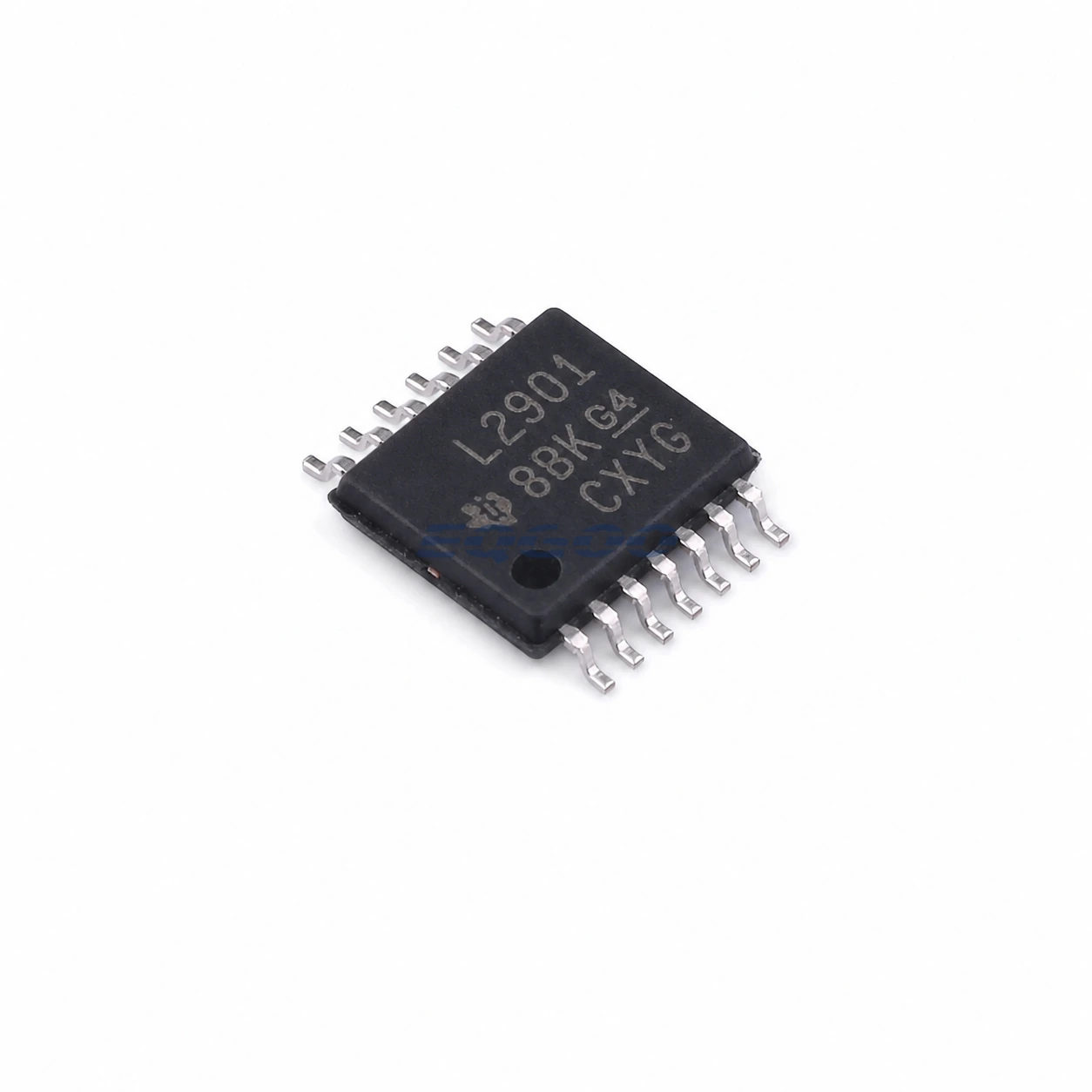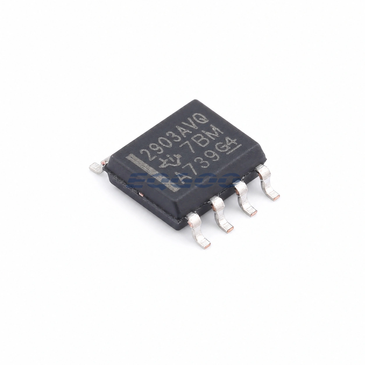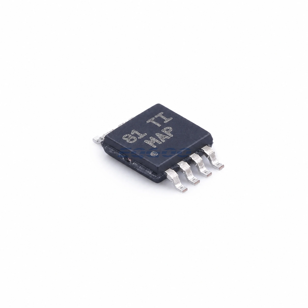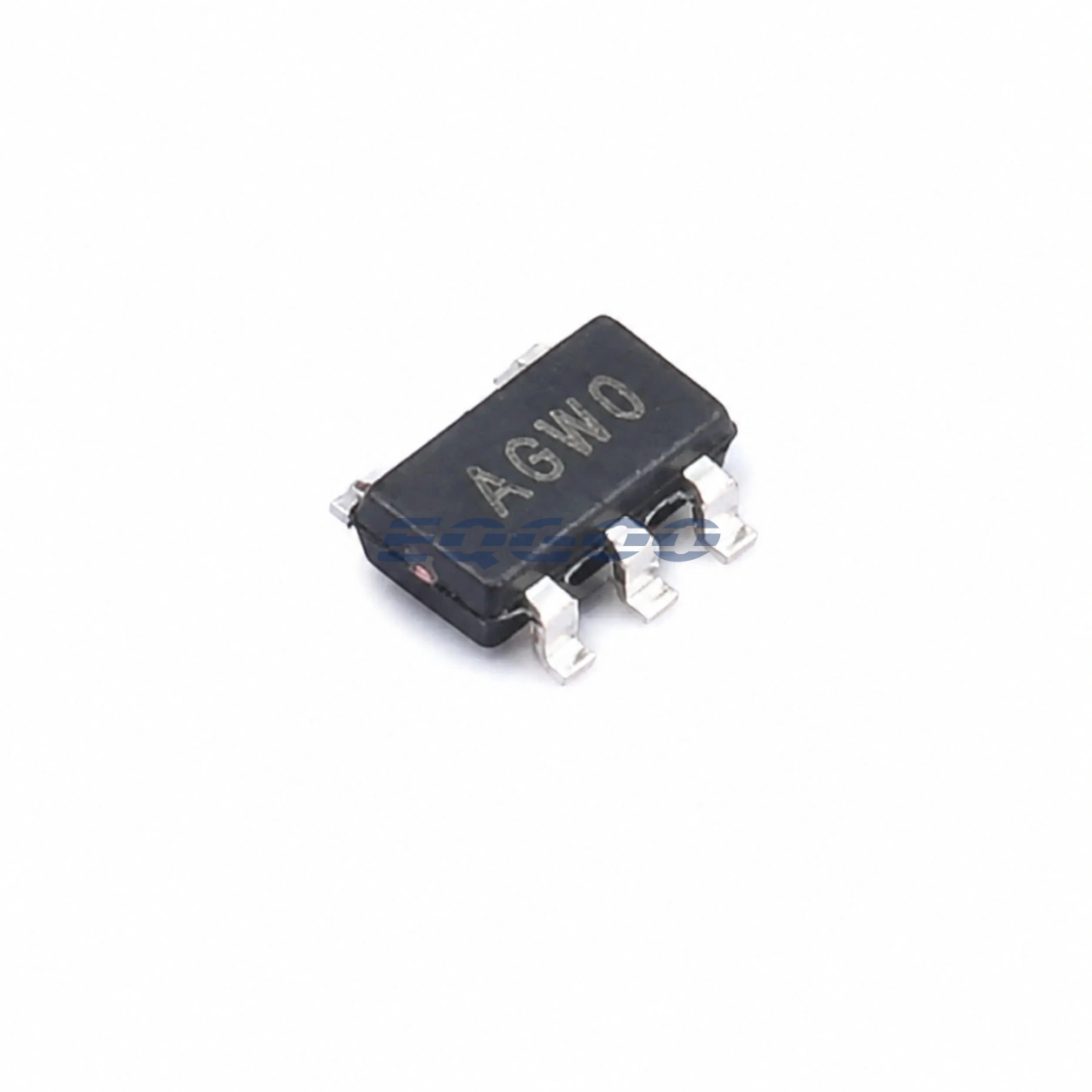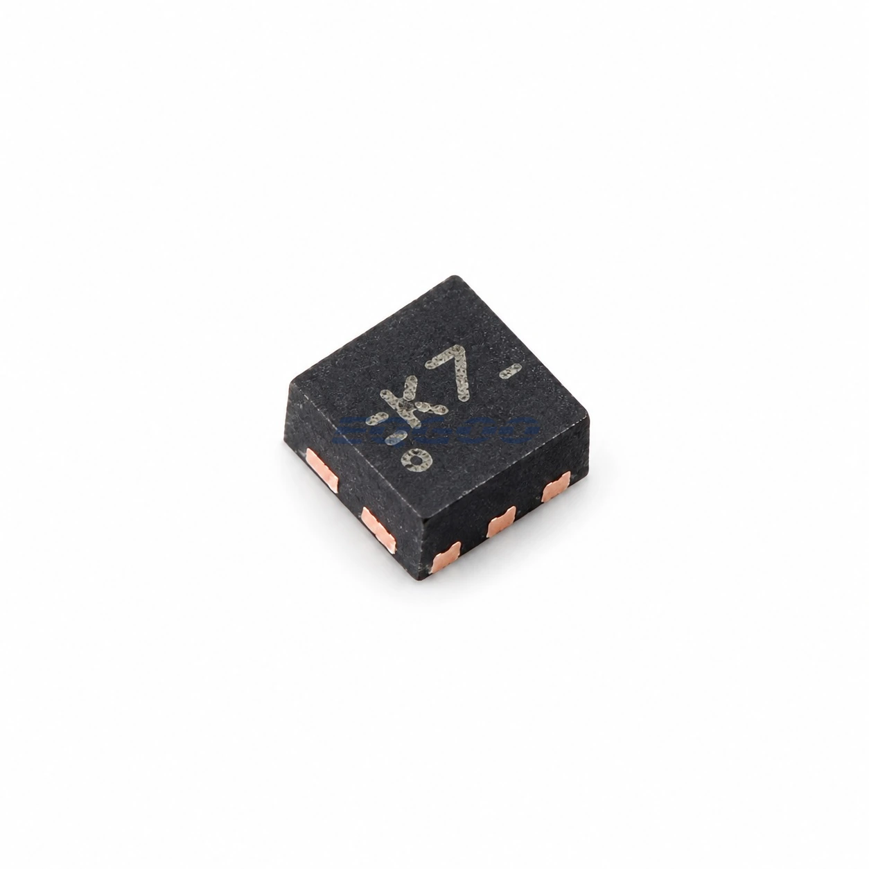
TLV6703QDSERQ1 is TI’s automotive TLV6703-Q1 comparator ordering option in a WSON-6(1.5×1.5) catalog package (TI drawing DSE, 6 pins). It combines an internal 400 mV reference, external-resistor-adjustable monitoring threshold and an open-drain output for voltage-status signalling.
Manufacturer-supported characteristics
| Selection parameter | Supported value | Condition or design meaning |
|---|---|---|
| Device function | Comparator with 400 mV integrated reference | External resistors determine monitored-voltage threshold |
| Supply-voltage range | 1.8–18 V | Normal device supply range |
| Reference accuracy at 25°C | 0.5% maximum | Not an unqualified whole-temperature accuracy figure |
| Reference accuracy over temperature | 1.0% maximum | Applies over the manufacturer’s specified temperature envelope |
| Quiescent current | 5.5 µA typical | Typical operating-current figure, not a guaranteed maximum |
| Internal hysteresis | 5.5 mV typical | Helps reject brief input fluctuations around the threshold |
| Propagation delay, high-to-low | 18 µs | VDD = 5 V, SENSE input overdrive 10 mV, RP = 10 kΩ, per TI timing table |
| Propagation delay, low-to-high | 29 µs | Same stated test setup; the two edge delays are not interchangeable |
| Output structure | Open drain | Requires correct pull-up voltage/current and interfacing |
| Output-voltage rating | Up to 18 V | Open-drain output rating; verify pull-up design constraints |
| Ambient grade | −40°C to +125°C | Automotive AEC-Q100 grade-1 device class |
| Package | WSON-6(1.5×1.5) | TI drawing DSE, 6 pins; check the exact landing pattern |
Threshold and output-interface considerations
The 400 mV reference is used with a resistor-divider network to select the voltage being monitored; it should not be described as a 400 mV supply-voltage operating minimum. The 0.5% at 25°C and 1.0% over temperature limits are different accuracy envelopes and should be evaluated under the intended temperature conditions.
The open-drain OUT signal is not a push-pull logic driver. Select a pull-up network appropriate to the host logic supply and output current. The typical 5.5 mV hysteresis helps reduce chatter near threshold crossings but does not guarantee immunity to every transient or board-level noise event. Under the manufacturer’s 5 V, 10 mV overdrive and 10 kΩ pull-up timing test, the high-to-low propagation delay is 18 µs while low-to-high is 29 µs. These are conditioned timings, not a general claim of sub-microsecond voltage-fault response.
For a dual general-purpose comparator without the TLV6703 integrated 400-mV reference, compare LM2903AVQDRQ1. The TLV6703-Q1 offers one reference-based voltage-detection channel and an open-drain output, while the LM2903AV-Q1 provides two independent open-collector comparators. Threshold circuitry, supply constraints, package and pin connections differ; they are not direct substitutes.
Exact ordering and RFQ
This ordering code uses six-pin WSON-6(1.5×1.5) (TI DSE drawing) rather than the SOT-23 package also available within the broader TLV6703 family. Match the landing pattern and confirm your sourcing requirements through HKEQGOO’s RFQ form.