Device Overview
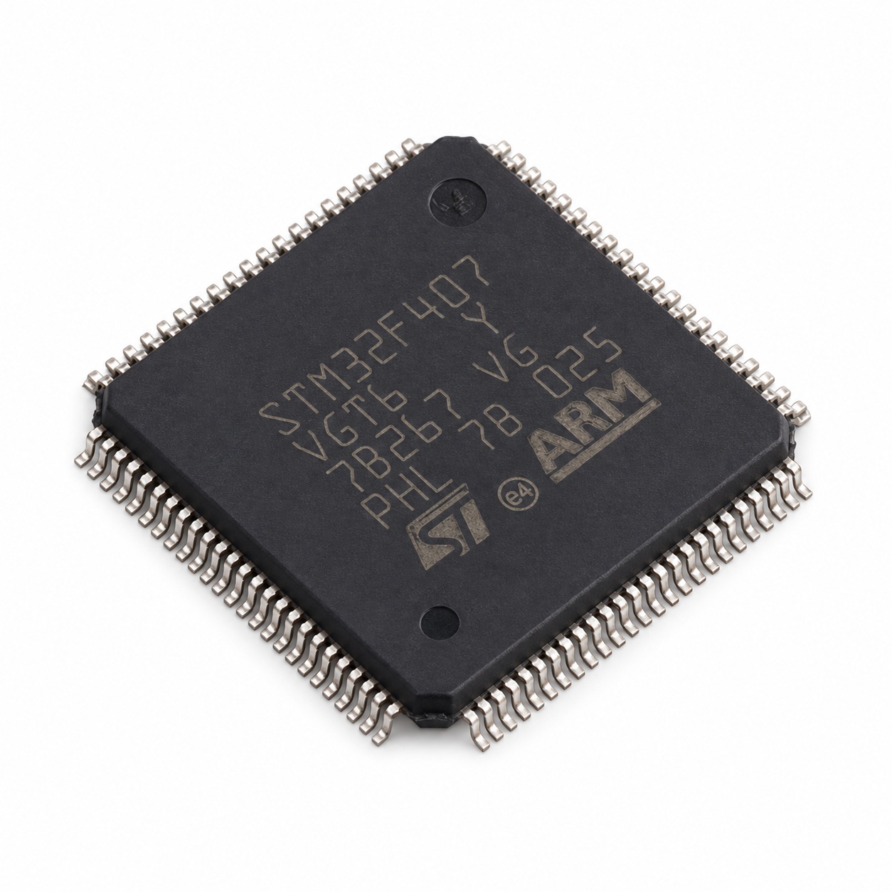
STM32F407VGT6 is the industrial-temperature LQFP100 orderable in STMicroelectronics’ STM32F407VG family. It combines a 168 MHz Arm Cortex-M4 core with single-precision FPU and DSP instructions, 1 MB of Flash, and up to 192 KB of SRAM plus 4 KB of backup SRAM. ST currently lists this exact orderable as active and in volume production.
Confirmed Technical and Ordering Data
| Parameter | Confirmed value | Scope / condition |
|---|---|---|
| Processor Core | Arm Cortex-M4 32-bit core with single-precision FPU and DSP instructions | |
| Clock | 168 MHz | maximum CPU frequency |
| Program Memory | 1 MB | Flash memory for the VG density |
| Ram | Up to 192 KB SRAM + 4 KB backup SRAM | family memory architecture for STM32F407VG; includes 64 KB CCM data RAM within SRAM resources |
| Interfaces | Ethernet MAC, USB OTG FS and HS/FS, CAN, SD/MMC, SPI/I2S, I2C and USART/UART interfaces | exact pin availability depends on the LQFP100 package |
| Analog Peripherals | Three 12-bit ADCs and two 12-bit DAC channels | family feature |
| Supply Voltage | 1.8 to 3.6 V | application supply and I/O range; datasheet notes a reduced-temperature 1.7 V condition with external supervisor |
| Temperature Grade | -40 to 85 °C | exact STM32F407VGT6 orderable grade |
| Package | LQFP-100 (14×14 mm) | exact orderable/package form |
| Temperature Range | -40 to 85 °C | exact orderable or manufacturer family grade |
Engineering Selection Guidance
The VGT6 suffix matters because it fixes both the 1 MB memory density and the 100-pin 14 x 14 mm LQFP package with a -40 °C to 85 °C ambient grade. The family provides Ethernet, USB OTG, CAN, SD/MMC and multiple serial interfaces, but the usable peripheral mix is constrained by the pin multiplexing of the 100-pin package, so interface-count decisions should be checked against the pinout rather than only the family feature list. The device also includes three 12-bit ADCs and two DAC channels. ST specifies a 1.8 V to 3.6 V application supply range; the datasheet’s lower 1.7 V condition is tied to a reduced-temperature/external-supervisor case and should not be generalized.
Procurement Notes
Manufacturer lifecycle/status evidence for this exact orderable is recorded as ACTIVE / volume production. Package identity is LQFP-100 (14×14 mm). Confirm final availability, lot/date-code requirements, and commercial terms through the RFQ process.
Lifecycle status does not indicate HKEQGOO stock, lead time, MOQ, or final availability.
For an STM32F407 MCU in the same LQFP-100 package with a smaller 512-KB Flash option, compare STM32F407VET6. This VGT6 orderable provides 1 MB of Flash; verify memory headroom and firmware image size.
For a 144-pin LQFP STM32F407 option with 512 KB Flash, compare STM32F407ZET6. The package has more pins and a different PCB footprint than this 100-pin, 1-MB-Flash VGT6 device.
For the same 1-MB Flash capacity in a 144-pin LQFP package, compare STM32F407ZGT6. The pin count and PCB footprint differ from this LQFP-100 variant; review the board design and peripheral allocation.