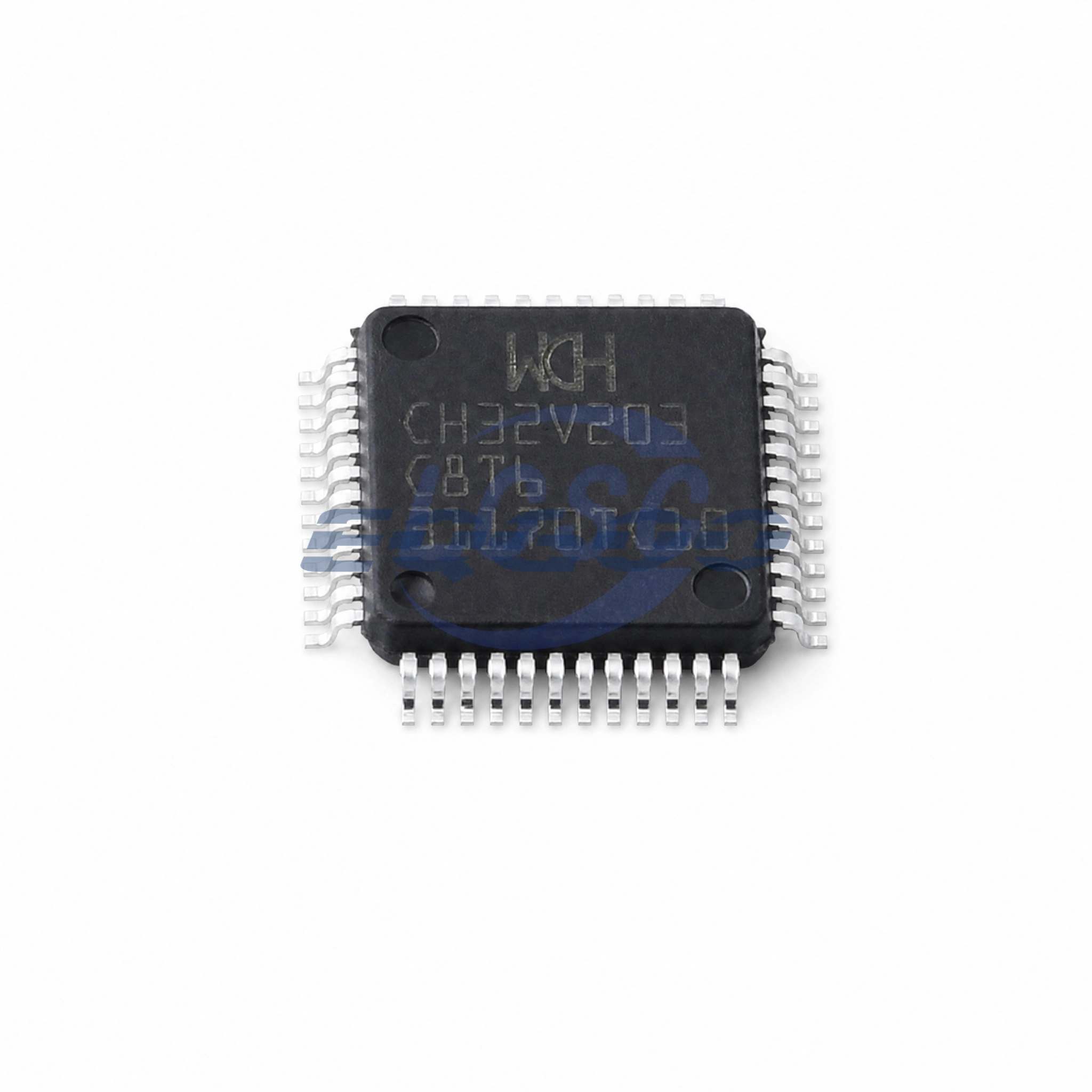
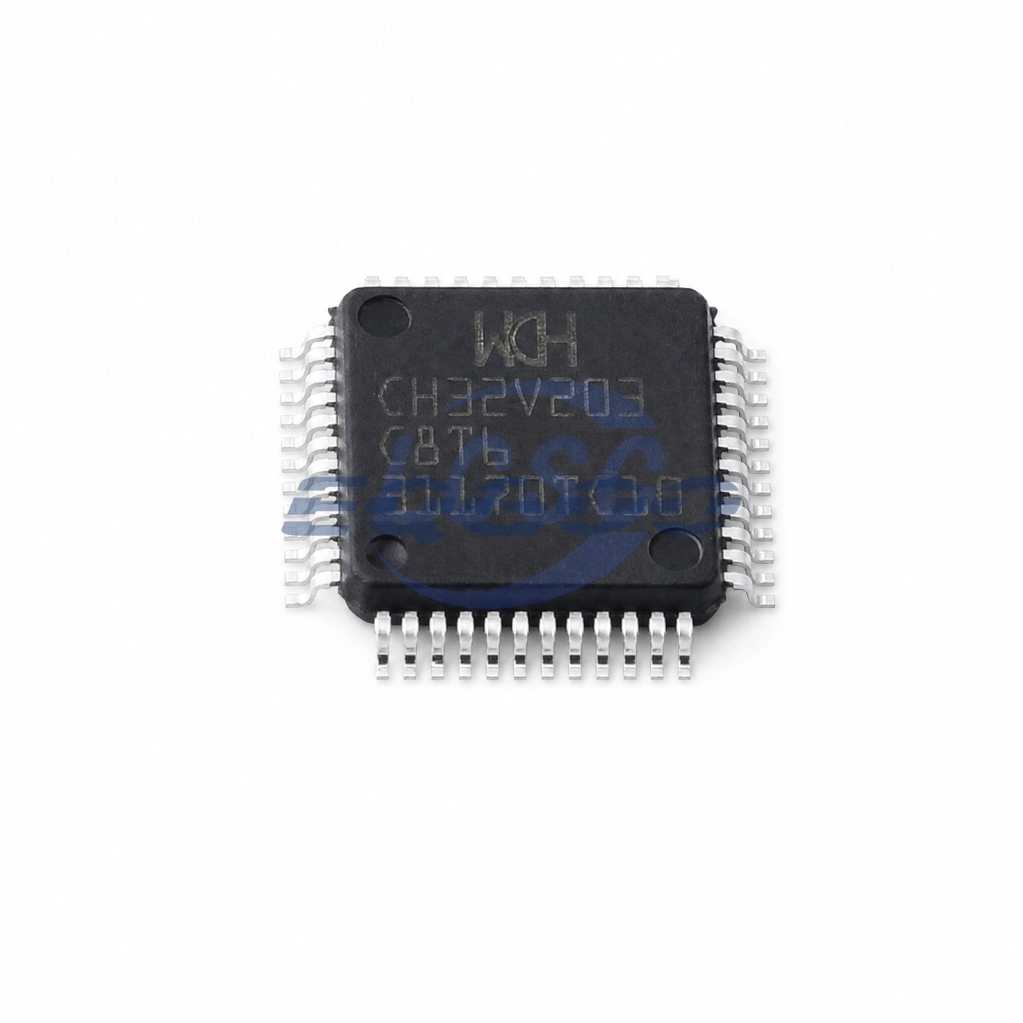
Key Selection Information
| Selection Parameter | Confirmed Information |
|---|---|
| Package | LQFP-48(7×7) |
| Supply voltage | 3.3V |
| CPU Core | RISC-V |
| Maximum CPU speed | 144MHz |
| Program memory | 64KB |
| Operating Temperature | -40℃~+85℃ |
| Number of I/O | 48 |
Product Overview
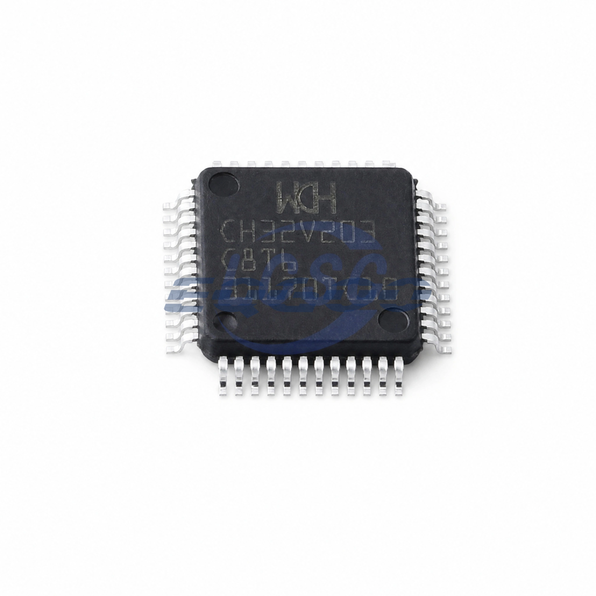
CH32V203C8T6 is a WCH microcontroller identified by the exact orderable code CH32V203C8T6. Its confirmed technical identity includes Supply voltage 3.3V, CPU Core RISC-V, Maximum CPU speed 144MHz, Program memory 64KB.
The exact device is described as: RISC-V 32 Bit 144MHz LQFP-48(7×7) Microcontrollers. Selection should be based on the exact package and the operating conditions required by the design, rather than on a nearby family member or a generic part number.
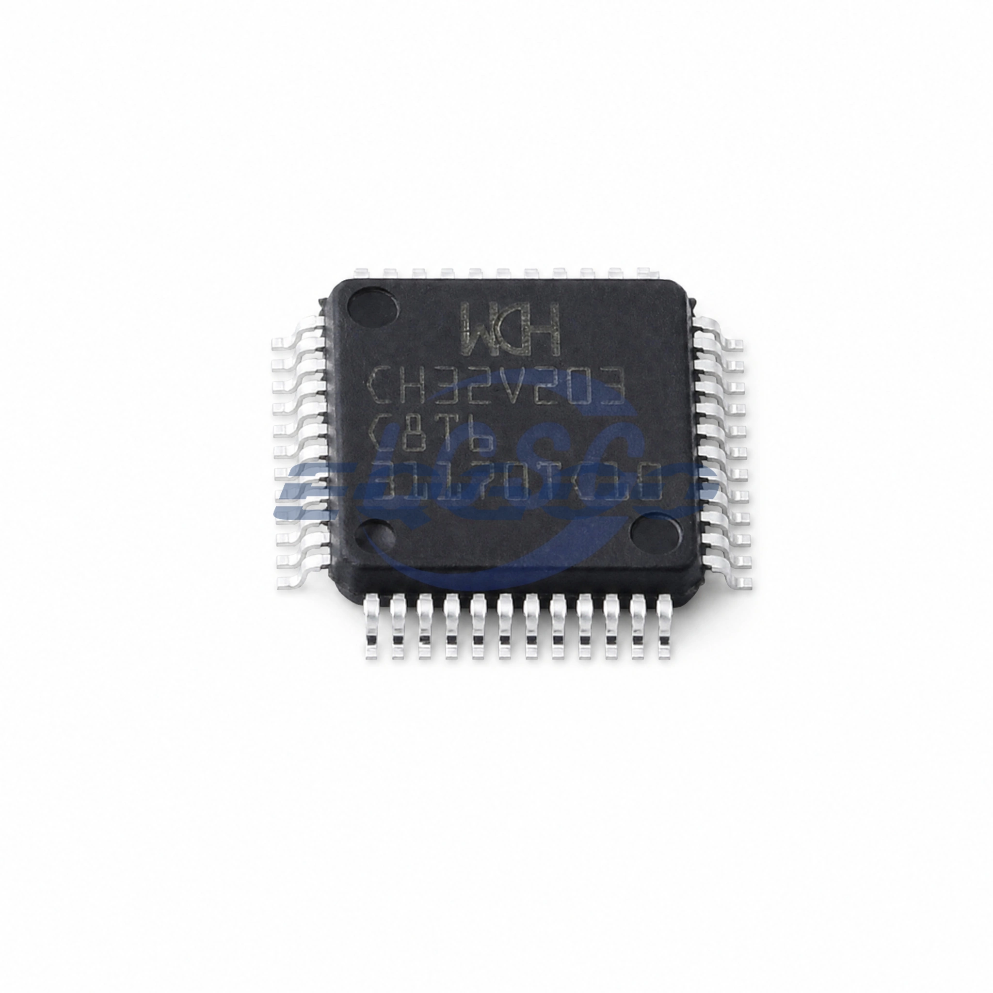
Technical Specifications
| Parameter | Value |
|---|---|
| Package | LQFP-48(7×7) |
| Supply voltage | 3.3V |
| CPU Core | RISC-V |
| Maximum CPU speed | 144MHz |
| Program memory | 64KB |
| Operating Temperature | -40℃~+85℃ |
| Number of I/O | 48 |
| ADC (Bit) | 12bit |
| Program Memory Type | FLASH |
| Core Size | 32 Bit |
| Oscillator Type | Built-in+External |
Exact-Part Selection Insight
The exact CH32V203C8T6 orderable code ties 64KB program memory to the LQFP-48(7×7) implementation and 48 listed I/O. Moving to a nearby family member can change memory capacity or pin availability, so the firmware memory map and PCB pinout should be checked together rather than treating the family name as interchangeable.
Selection Notes
- Package: LQFP-48(7×7)
- Supply voltage: 3.3V
- CPU Core: RISC-V
- Maximum CPU speed: 144MHz
- Program memory: 64KB
Application Fit
This exact part is appropriate for designs that require a microcontroller with the confirmed package and electrical/function parameters above. Final fit depends on the surrounding circuit, interface, thermal and mechanical requirements of the target design.
Design Considerations
Confirm the available supply rail stays inside the stated operating range, including startup and transient conditions.
Confirm memory size, available I/O, clocking and required peripheral set for the exact orderable device before freezing firmware and PCB pinout.
Use the exact LQFP-48(7×7) footprint/package definition when checking PCB land pattern, assembly clearance and sourcing equivalence.
Quality & Verification Support
Third-party inspection or testing can be arranged according to customer requirements. Testing fees are borne by the buyer. Additional verification requirements can be discussed before shipment. After an order is placed, physical product, label, packaging, and Date Code photos may be provided where appropriate.
Request a Quote
To request a quotation, provide the manufacturer part number, required quantity, destination, target Date Code if applicable, and any testing or inspection requirements.
Related Engineering Resources
- CH32V203C8T6 Datasheet (PDF) ??manufacturer datasheet mirrored by LCSC and verified as the original technical document.
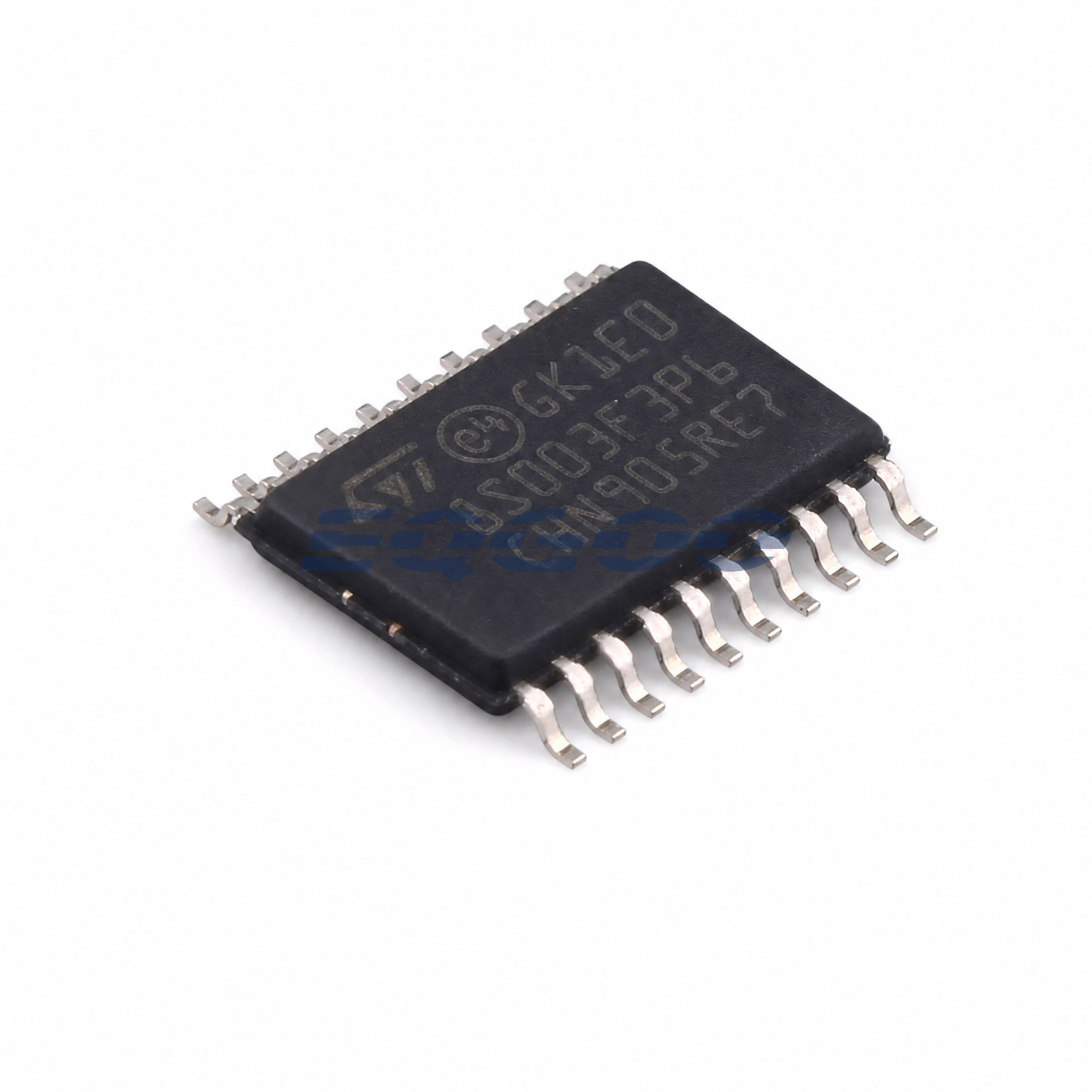
For a 20-pin TSSOP layout instead of this 48-pin LQFP layout, compare the WCH CH32V203 family variant CH32V203F8P6. Both orderables specify 64 KB of Flash, but the lower pin-count package exposes fewer I/O options. Revalidate the actual peripheral pins, USB signals, board routing and firmware before choosing a different package.