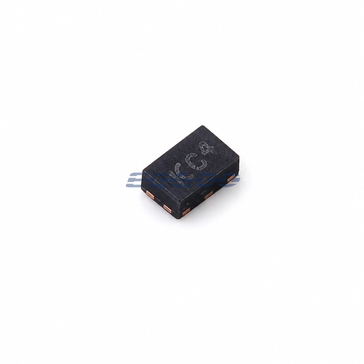
Key Selection Information
| Selection Parameter | Confirmed Information |
|---|---|
| Switch type | Broadband SPDT RF switch |
| Frequency range | 0.05 GHz to 9 GHz |
| Insertion loss | 0.16 dB at 1 GHz product-detail value |
| Isolation | 46 dB at 1 GHz product-detail value |
| RF input power | Up to 30 dBm |
| Supply voltage | 1.65 V to 3.6 V |
| Control | GPIO with on-chip logic |
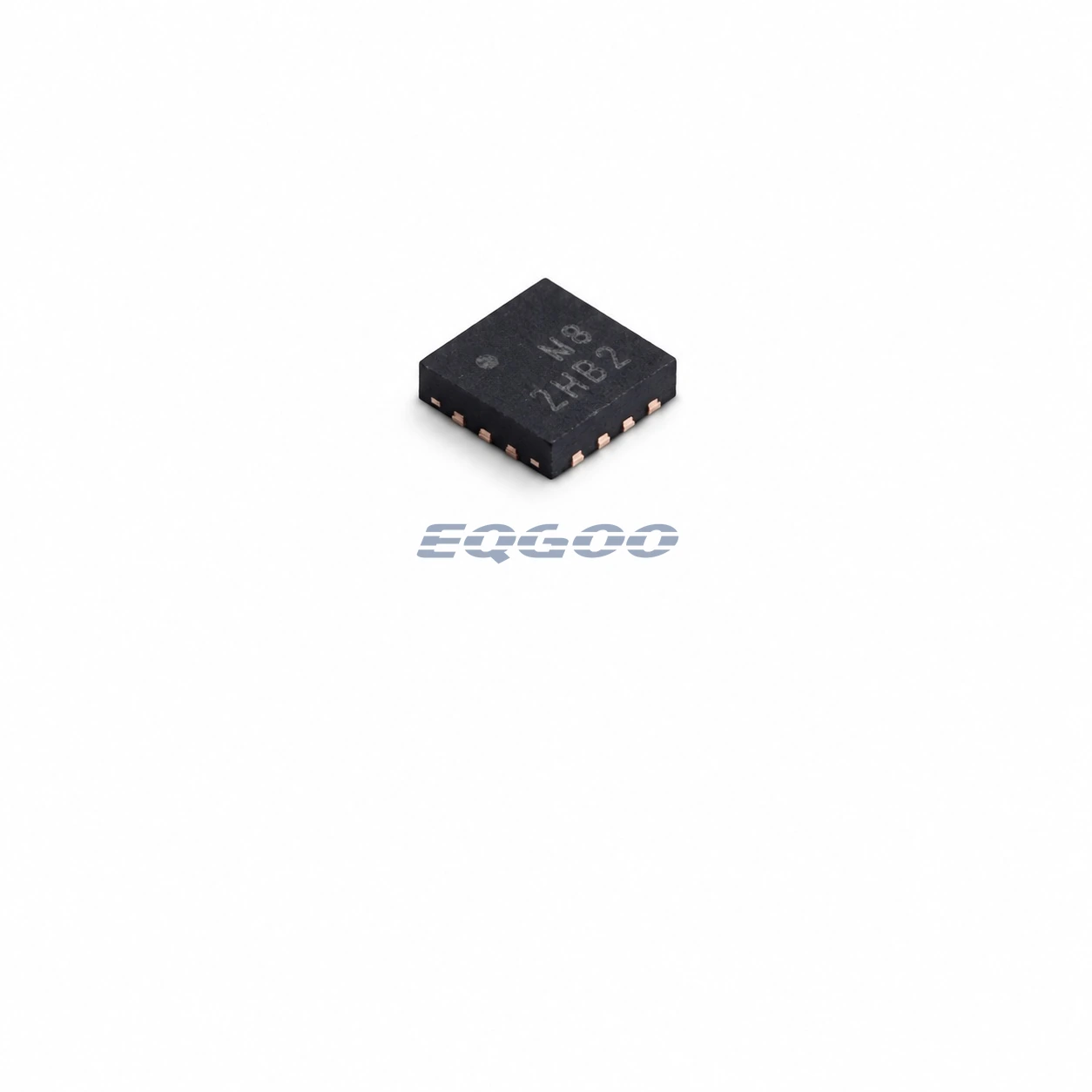
| Package | PG-TSNP-6-10, 0.7 × 1.1 mm |
Product Overview
The BGS 12WN6 E6327 is the E6327 sales-product version of Infineon’s BGS12WN6 broadband SPDT RF switch; the current full OPN is BGS12WN6E6327XTSA1. Infineon positions the device for WiFi, Bluetooth, UWB and cellular switching with a 0.05 GHz to 9 GHz frequency range.
The part combines a very small 0.7 × 1.1 mm TSNP package with low insertion loss and high isolation. Infineon’s current product detail lists 0.16 dB insertion loss and 46 dB isolation at 1 GHz, while the 2026 datasheet extends the RF characterization out to 9 GHz. That extended upper-frequency coverage is a meaningful distinction from older 6 GHz BGS12SN6 designs.
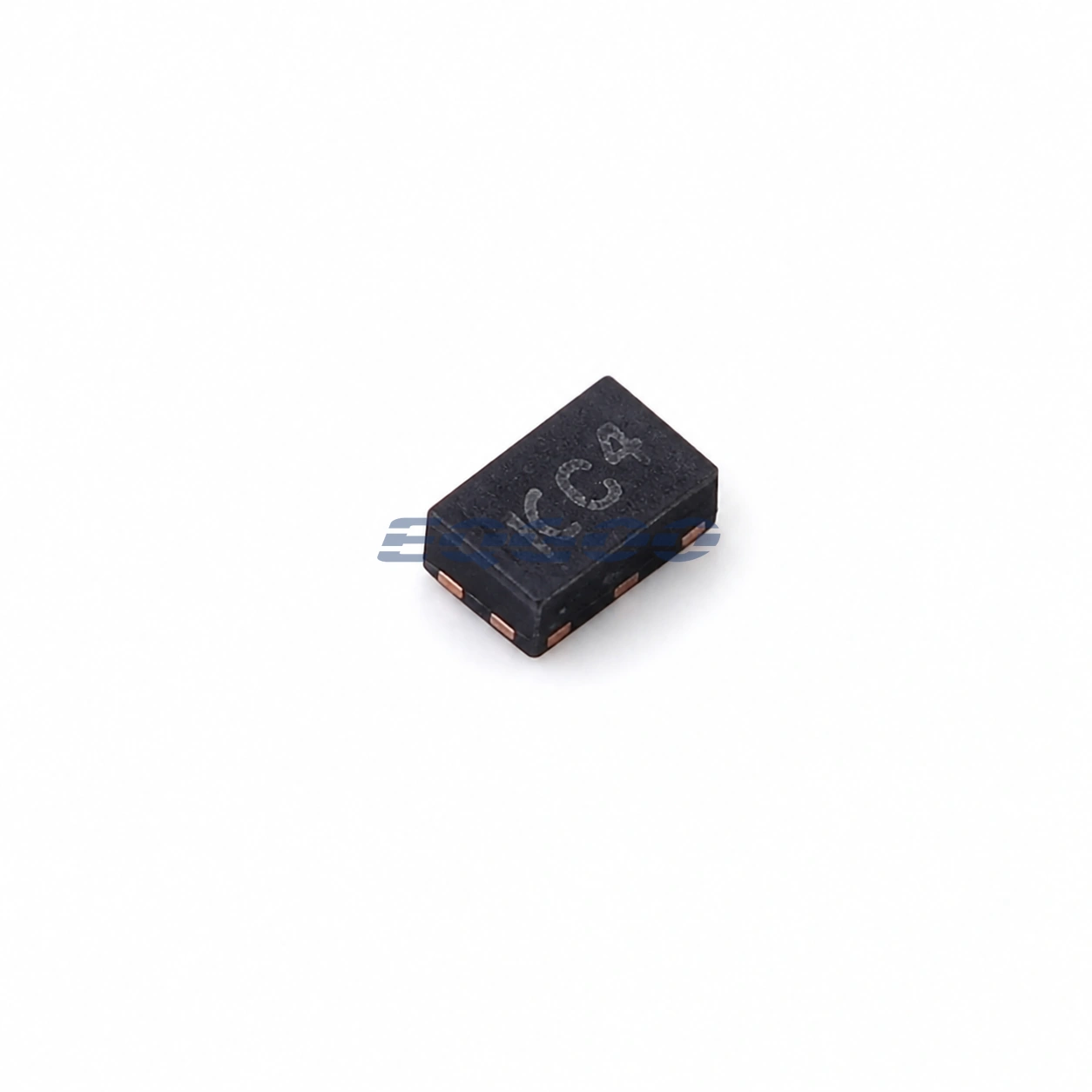
Technical Specifications
| Parameter | Confirmed Information |
|---|---|
| Topology | SPDT |
| Control interface | GPIO |
| Frequency range | 0.05 GHz to 9 GHz |
| Insertion loss at 1 GHz | 0.16 dB product-detail value |
| Isolation at 1 GHz | 46 dB product-detail value |
| RF input power | Up to 30 dBm |
| Supply voltage | 1.65 V to 3.6 V |
| Package | PG-TSNP-6-10 |
| Package size | 0.7 × 1.1 mm |
| Package height | Approximately 0.37 mm |
| DC blocking | Not required when no DC is applied to RF lines |
| Full OPN | BGS12WN6E6327XTSA1 |
| Product status | Active and preferred |
Design Considerations
The extended 9 GHz coverage should be evaluated with the frequency-specific loss and isolation curves, not only the 1 GHz product-detail values. At several gigahertz, PCB launch geometry, ground return and line discontinuities can dominate the practical insertion loss.
The official package is PG-TSNP-6-10 rather than a generic DFN-6. Use the Infineon land pattern and package height when checking footprint compatibility or replacing an older TSNP variant.
Related Engineering Resources
Quality & Verification Support
Third-party inspection or testing can be arranged according to customer requirements. Testing fees are borne by the buyer. Additional verification requirements can be discussed before shipment. After an order is placed, physical product, label, packaging, and Date Code photos may be provided where appropriate.
Request a Quote
To request a quotation, provide the manufacturer part number, required quantity, destination, target Date Code if applicable, and any testing or inspection requirements.