Key Selection Information
| Selection Parameter | Confirmed Information |
|---|---|
| Function | High-linearity SPDT RF switch |
| Frequency range | 0.5 GHz to 6.0 GHz |
| Insertion loss | 0.16 dB at 1 GHz product-detail value |
| Isolation | 39 dB at 1 GHz product-detail value |
| RF power handling | Up to 38 dBm feature value |
| IIP3 | 75 dBm |
| Supply voltage | 1.8 V to 3.6 V |
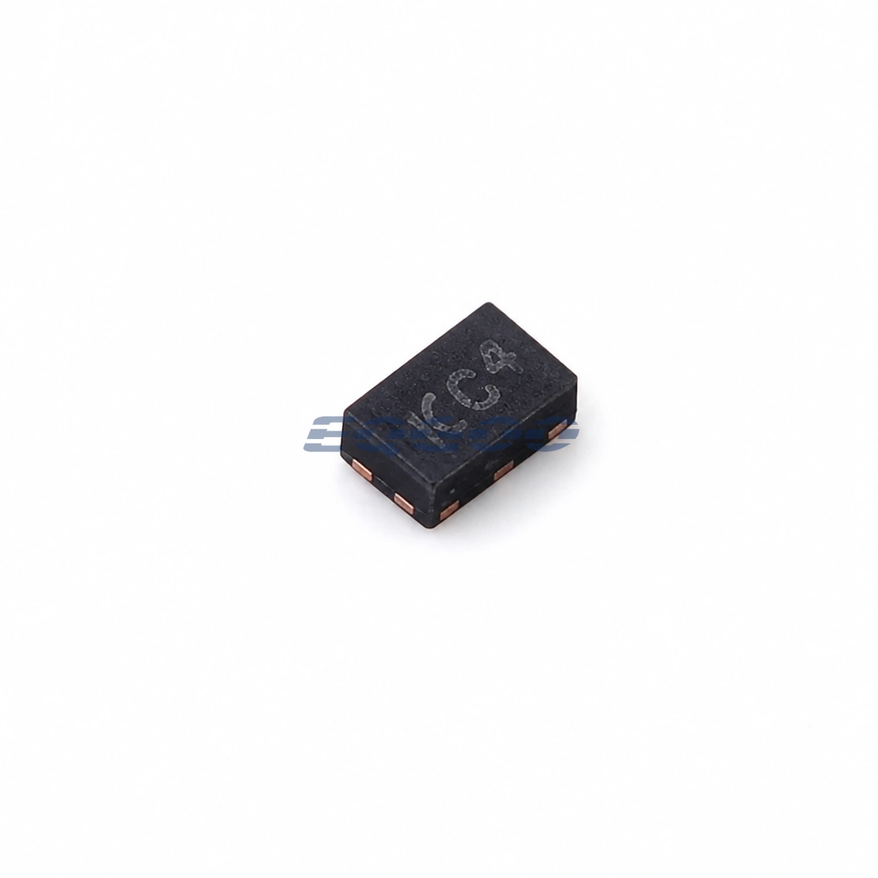
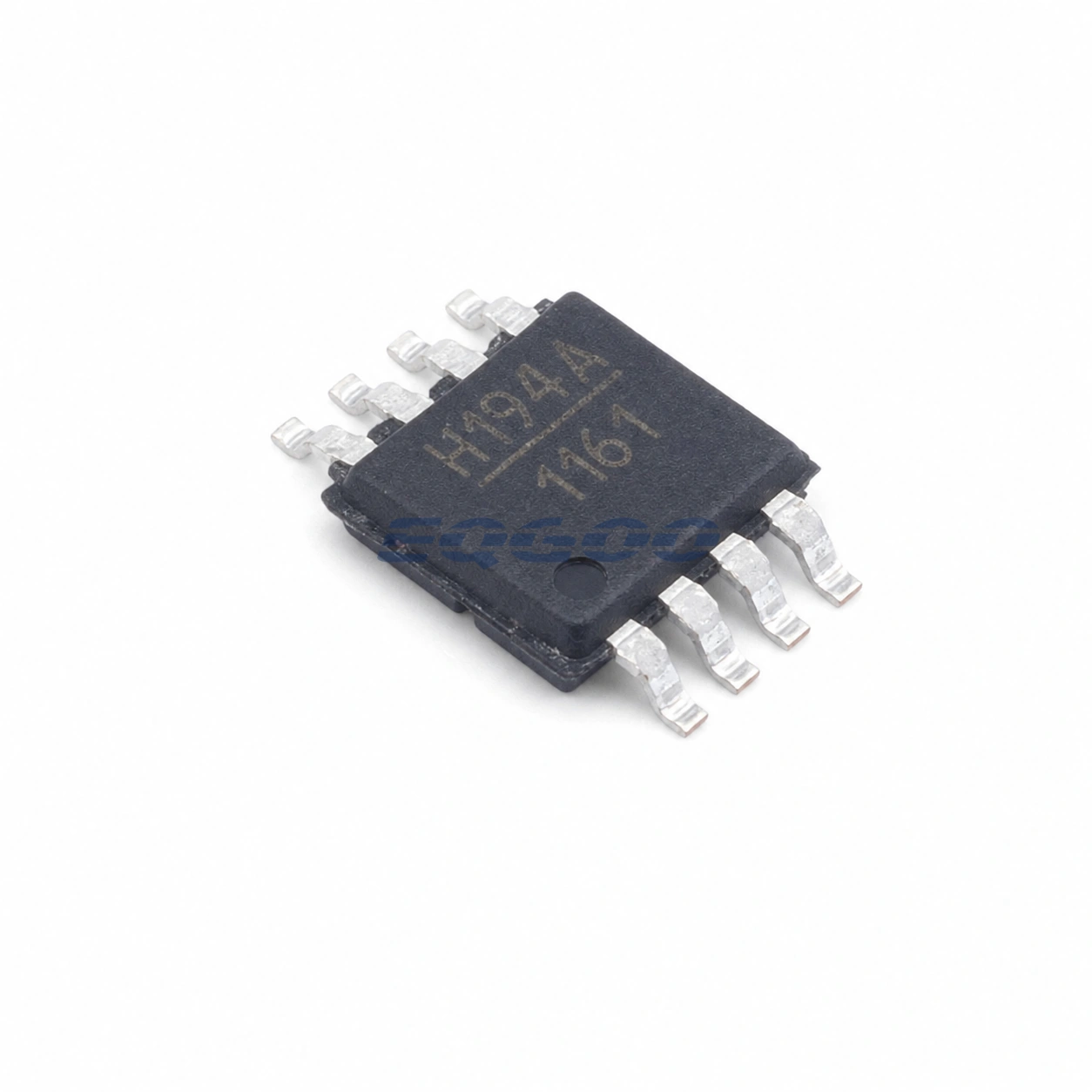
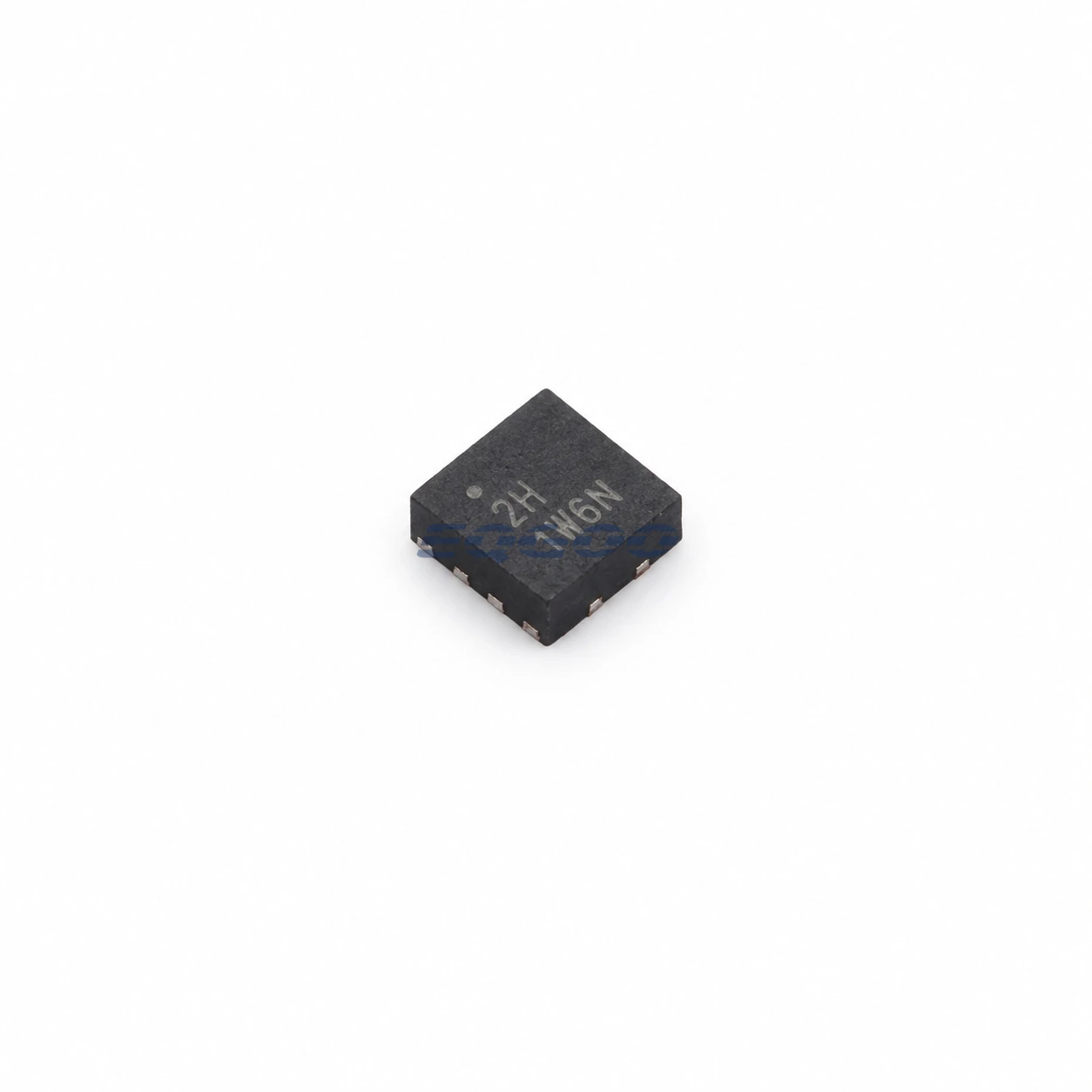
| Package | TSNP-10-1, 1.1 × 1.5 mm |
Product Overview
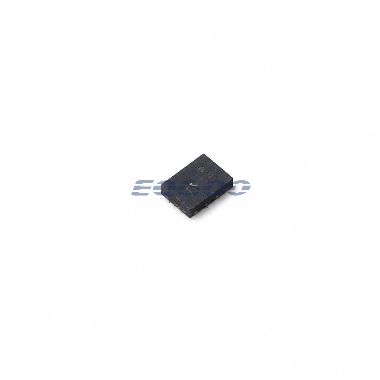
The BGS 12PN10 E6327 is Infineon’s sales-product identity for the BGS12PN10 high-power SPDT RF switch; the current full OPN is BGS12PN10E6327XTSA1. It is designed for high-linearity transmit/receive switching from 0.5 GHz to 6 GHz and remains active in Infineon’s current portfolio.
The device is notable for combining very low insertion loss with high transmit-power capability. Infineon lists 0.17 dB insertion loss at 0.9 GHz with 38 dBm input and 0.22 dB at 1.9 GHz with the same input condition, while the family product page shows 75 dBm IIP3. This makes power level and operating frequency inseparable from the insertion-loss specification.
Technical Specifications
| Parameter | Confirmed Information |
|---|---|
| Switch topology | SPDT |
| Control interface | GPIO / CMOS / TTL compatible |
| Frequency range | 0.5 GHz to 6.0 GHz |
| Insertion loss at 1 GHz | 0.16 dB product-detail value |
| Isolation at 1 GHz | 39 dB product-detail value |
| RF power handling | 38 dBm feature value |
| Absolute maximum RF input | 40 dBm CW at 900 MHz under documented condition |
| IIP3 | 75 dBm |
| Supply voltage | 1.8 V to 3.6 V |
| DC blocking | Not required when no external DC is applied to RF ports |
| Package | TSNP-10-1, 1.1 × 1.5 mm |
| Full OPN | BGS12PN10E6327XTSA1 |
| Product status | Active |
Design Considerations
The loss values are frequency- and power-condition dependent. Use the figure for the intended RF band and expected transmit level rather than applying the 1 GHz product-detail number across the entire 6 GHz range.
The official package is TSNP-10-1, not a generic DFN-10. That distinction should be preserved in footprint selection because package naming, pad layout and assembly data come from the Infineon TSNP definition.
Related Engineering Resources
Quality & Verification Support
Third-party inspection or testing can be arranged according to customer requirements. Testing fees are borne by the buyer. Additional verification requirements can be discussed before shipment. After an order is placed, physical product, label, packaging, and Date Code photos may be provided where appropriate.
Request a Quote
To request a quotation, provide the manufacturer part number, required quantity, destination, target Date Code if applicable, and any testing or inspection requirements.