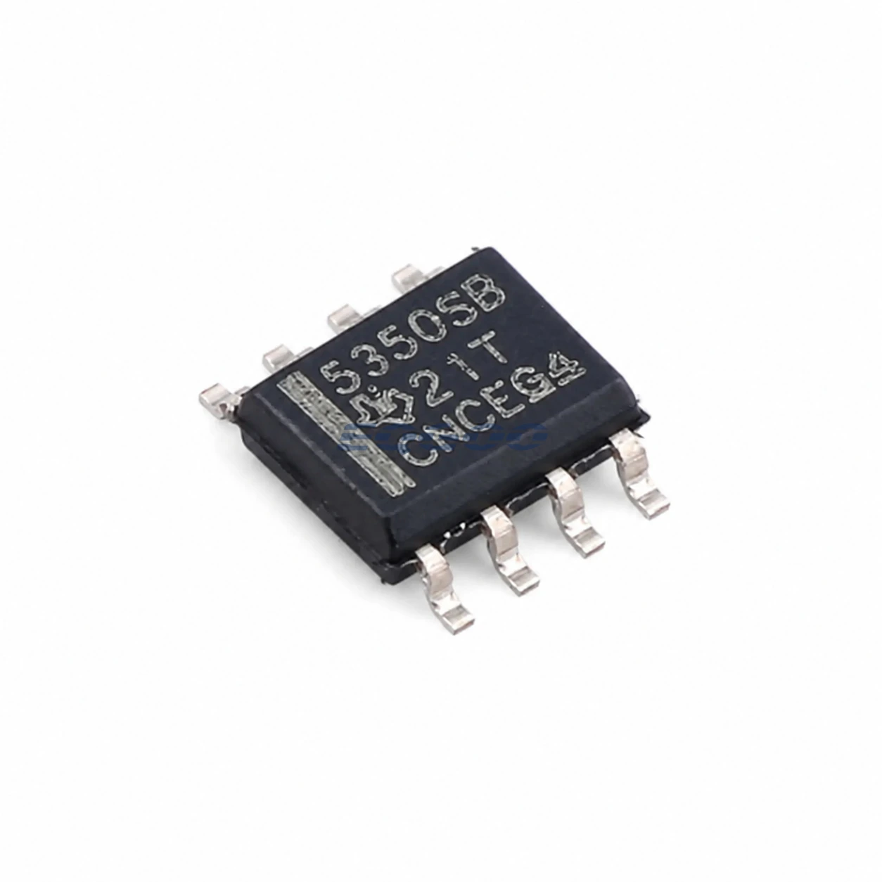

Key Selection Information
| Selection Parameter | Confirmed Information |
|---|---|
| Variant | UCC5350SB: split output with 8 V UVLO |
| Drive Strength | 8.5 A typical source / 10 A typical sink family table |
| Isolation Package | SOIC (D), 8 pins; 3 kVRMS-class D-package isolation |
| CMTI | 100 kV/µs minimum |
| Timing | 60 ns typical propagation delay |
| Input Supply | 3 V to 15 V |
| Driver Supply | Up to 33 V |
| Exact Package / Packing | SOIC (D), 8 pins; 2500-piece large tape and reel; active order code |
Product Overview
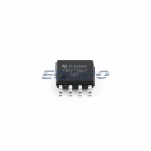
UCC5350SBDR is the split-output, 8 V-UVLO UCC5350SB orderable variant. Separate source and sink output pins let the designer use different turn-on and turn-off gate resistors without adding steering diodes, which is useful when dv/dt and turn-off robustness require asymmetric gate shaping.
The SB variant is listed with 8.5 A typical source and 10 A typical sink capability, 100 kV/µs minimum CMTI and about 60 ns typical propagation delay. The D package provides the compact 4 mm creepage-format option; wider DWV family packages are a different isolation/footprint choice.
TI’s current part-detail page lists UCC5350SBDR as active in SOIC-8 D, −40°C to +125°C, 2500-piece large tape-and-reel packaging.
For related devices, see HKEQGOO’s Isolators – Gate Drivers category.
Technical Specifications
| Parameter | Verified Information |
|---|---|
| Manufacturer | Texas Instruments |
| Exact MPN | UCC5350SBDR |
| Variant | UCC5350SB: split output with 8 V UVLO |
| Drive Strength | 8.5 A typical source / 10 A typical sink family table |
| Isolation Package | SOIC (D), 8 pins; 3 kVRMS-class D-package isolation |
| CMTI | 100 kV/µs minimum |
| Timing | 60 ns typical propagation delay |
| Input Supply | 3 V to 15 V |
| Driver Supply | Up to 33 V |
| Exact Package / Packing | SOIC (D), 8 pins; 2500-piece large tape and reel; active order code |
| Manufacturer Status | Active / Production |
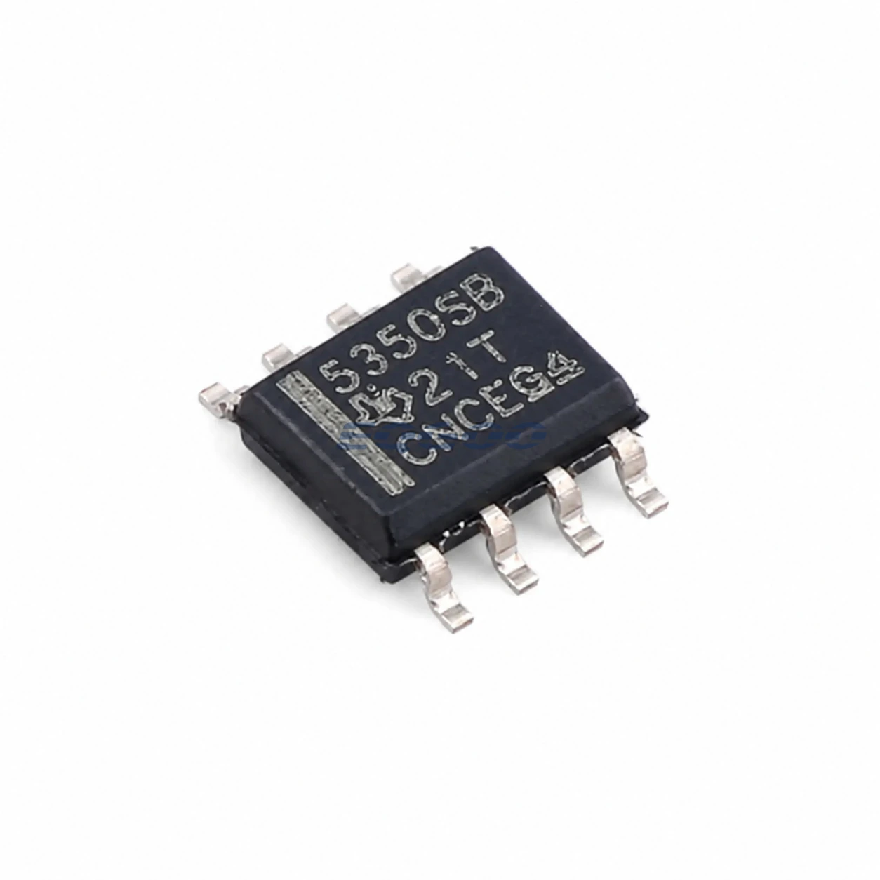
| Part Marking | UCC5350SB family marking per TI package data |
Functional Highlights
Split outputs make gate-shaping explicit
Independent source/sink paths allow a slower controlled turn-on and a faster turn-off, or vice versa, without the nonlinear behavior of external steering diodes. Gate resistors still must be selected from switch charge, loop inductance and EMI measurements.
8 V UVLO is part of the SB identity
The lower UVLO supports lower gate-drive rails than 12 V variants. The designer must ensure the chosen MOSFET/SiC device is fully enhanced at the intended drive voltage and fault conditions.
Design Considerations
- Keep source and sink gate paths short and place their resistors near the power switch/driver loop as appropriate.
- Confirm 8 V UVLO matches the power transistor’s safe minimum gate voltage; lower threshold is not automatically better.
- Use D-package creepage/working-voltage limits for the actual isolation requirement; do not assume the wider DWV family rating.
Product Status and Exact Order Code
Manufacturer status: Active / Production
Texas Instruments lists UCC5350SBDR as Active orderable part; SOIC (D), 8 pins; 2500-piece large tape and reel; Level-2-260C-1 YEAR; −40°C to +125°C.
Related Engineering Resources
Quality & Verification Support
Third-party inspection or testing can be arranged according to customer requirements. Testing fees are borne by the buyer. Additional verification requirements can be discussed before shipment. After an order is placed, physical product, label, packaging, and Date Code photos may be provided where appropriate.
Request a Quote
To request a quotation, provide the manufacturer part number, required quantity, destination, target Date Code if applicable, and any testing or inspection requirements.