Device Overview
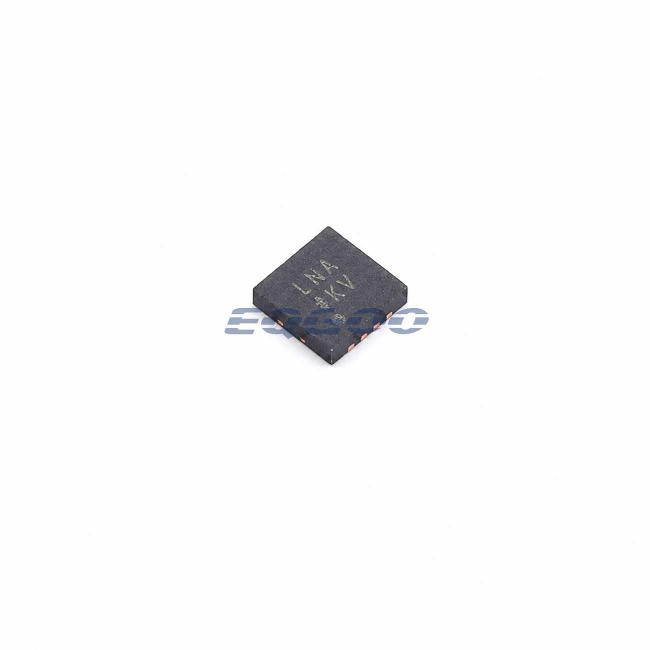
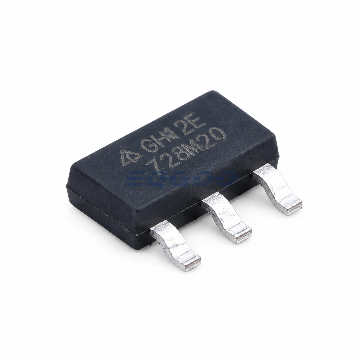
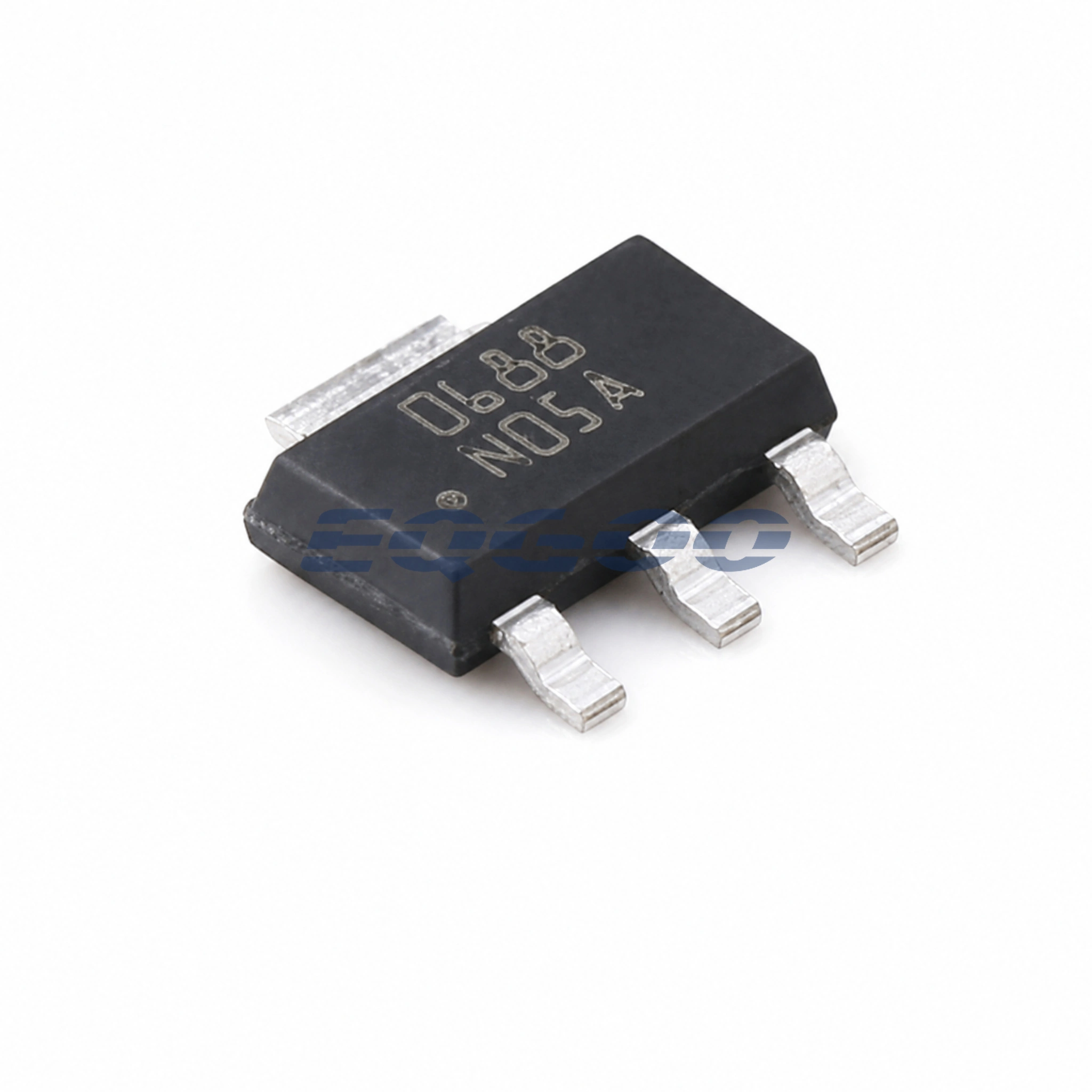
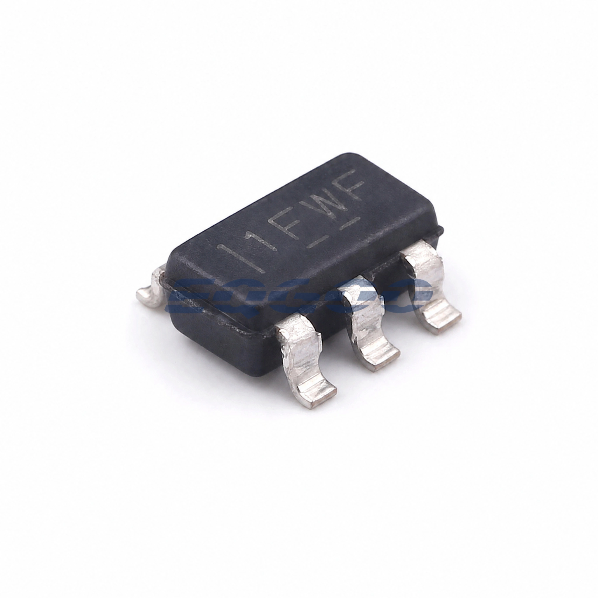
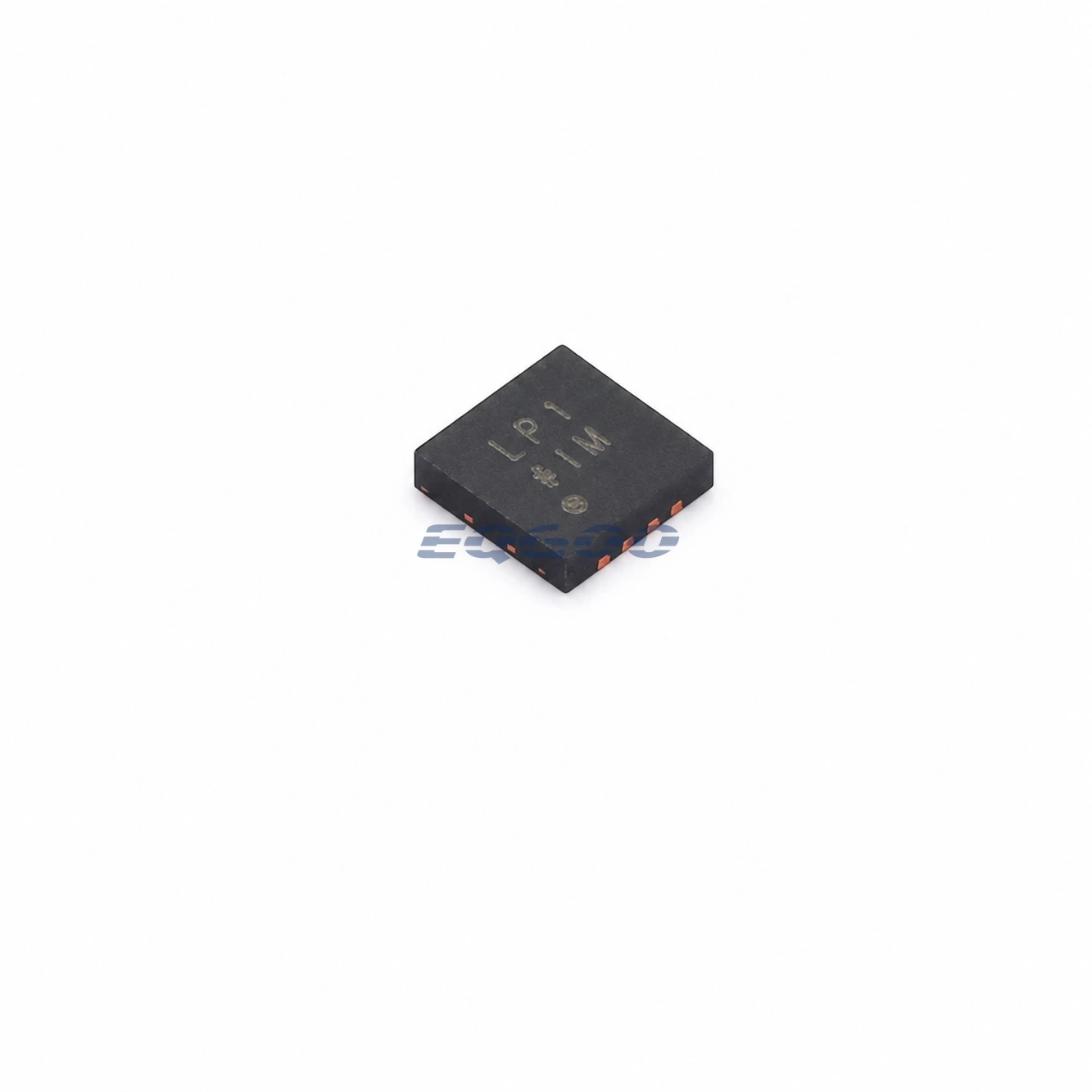
ADM7172ACPZ-5.0-R7 is the fixed 5.0 V, 2 A member of Analog Devices’ ADM7172 ultralow-noise CMOS LDO family in an 8-lead 3 mm x 3 mm LFCSP. It is intended for low-noise analog, converter, RF, and clock rails where output noise, transient response, headroom, and thermal dissipation all affect the design.
Key Selection Information
| Parameter | Verified Information |
|---|---|
| Manufacturer | Analog Devices |
| Exact MPN | ADM7172ACPZ-5.0-R7 |
| Fixed output voltage | 5.0 V |
| Family input operating range | 2.3 V to 6.5 V; the fixed 5.0 V orderable still requires enough VIN headroom above 5.0 V to regulate |
| Maximum load current | 2 A |
| Output noise | 5 µV RMS, 100 Hz to 100 kHz; specified independent of output voltage |
| No-load ground current | 0.7 mA typical |
| Shutdown current | 0.25 µA at VIN = 5 V |
| Transient-response reference | 1.5 µs for a 1 mA to 1.5 A load step |
| Output capacitor | Stable with a 4.7 µF ceramic output capacitor |
| Package | 8-lead LFCSP, 3 mm x 3 mm, exposed pad |
| Manufacturer lifecycle | Recommended for new designs |
Engineering Selection Notes
The family’s 2.3 V minimum input does not mean this exact 5.0 V version can regulate from 2.3 V. A fixed 5.0 V output requires VIN above the programmed output by the dropout/headroom needed at the actual load current.
The 5 µV RMS noise specification is defined over 100 Hz to 100 kHz and is independent of output voltage. That makes this orderable useful for noise-sensitive 5 V rails, but supply ripple, PCB grounding, output capacitance, and load transients still determine system-level performance.
Analog Devices quotes 172 mV dropout at 2 A for a 3 V output as a family characterization point. That number should not be copied as an unconditional exact-5 V dropout specification; use the output-specific curves and real VIN/VOUT margin when checking a 2 A design.
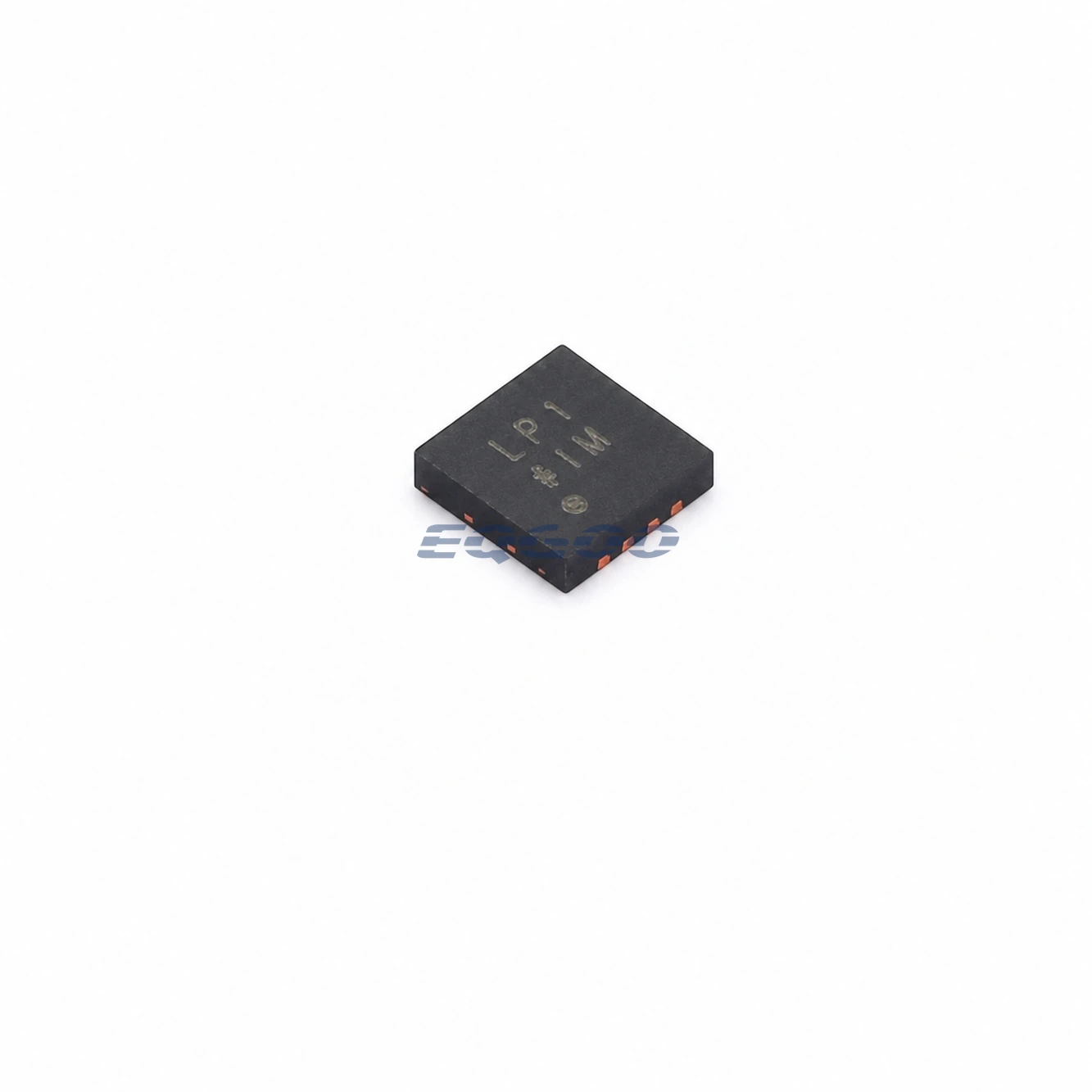
For an analog rail that requires a fixed 3.3 V output instead of this 5.0 V version, compare ADM7172ACPZ-3.3-R7. Both are rated as 2 A ADM7172-family LDO orderables in 8-lead LFCSP packages, but they have different output-voltage setpoints. Confirm available VIN headroom and regulator power dissipation rather than treating the parts as interchangeable without checking the load.
Official Engineering Resources
Quality & Verification Support
Third-party inspection or testing can be arranged according to customer requirements. Testing fees are borne by the buyer. Additional verification requirements can be discussed before shipment.
Request a Quote
For ADM7172ACPZ-5.0-R7 sourcing, provide the required quantity, destination, target Date Code if applicable, and any inspection or testing requirements.