Key Selection Information
| Selection Parameter | Confirmed Information |
|---|---|
| Function | Envelope detector plus TruPwr RMS detector |
| Frequency range | DC to 6 GHz |
| Input power dynamic range | 47 dB |
| Envelope bandwidth | 130 MHz |
| Envelope delay | 2 ns |
| Supply voltage | 4.75 V to 5.25 V |
| Typical current | 21.5 mA |
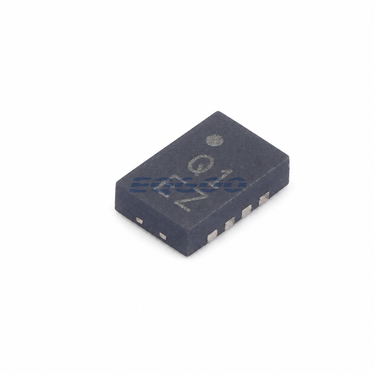
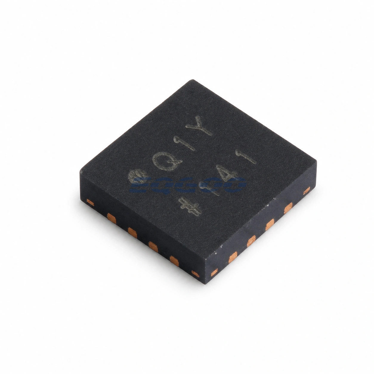
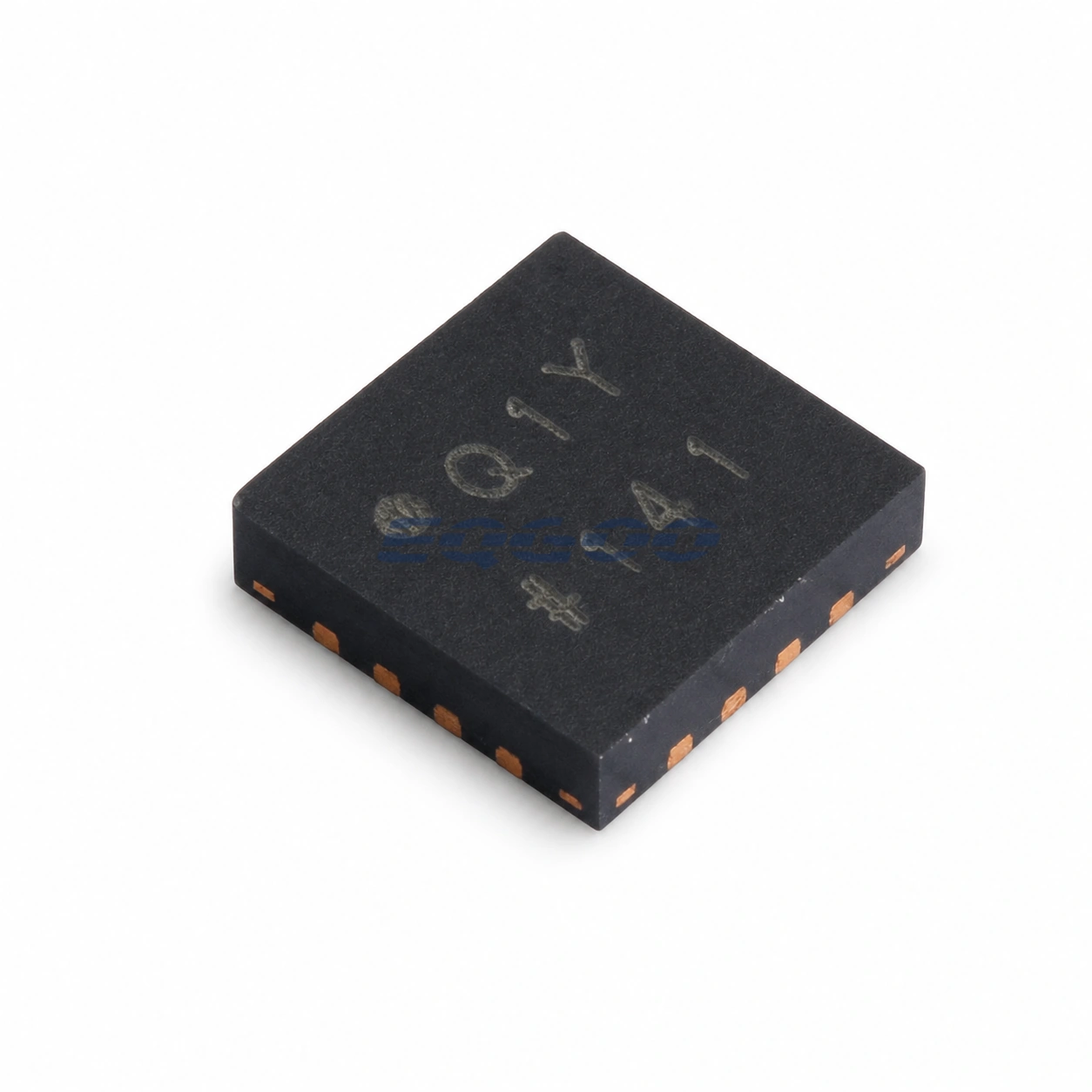
| Package | 16-lead LFCSP, 3 × 3 mm |
Product Overview
The ADL5511ACPZ-R7 combines two different RF measurement outputs in one device: a fast envelope output proportional to instantaneous input voltage and a separate true-rms output that reports signal power independently of peak-to-average ratio. It operates from dc to 6 GHz with 47 dB input power dynamic range.
This dual-output architecture is the key exact-part value. The envelope path provides 130 MHz bandwidth and only 2 ns delay, making it suitable for tracking fast amplitude changes in envelope-tracking or PA-linearization systems, while the rms path can simultaneously monitor true signal power.
Technical Specifications
| Parameter | Confirmed Information |
|---|---|
| RF input range | DC to 6 GHz |
| Input power dynamic range | 47 dB |
| Output types | Envelope and TruPwr RMS |
| Envelope bandwidth | 130 MHz |
| Envelope delay | 2 ns |
| RMS conversion gain at 900 MHz | 1.9 V/V rms |
| Envelope conversion gain at 900 MHz | 1.46 V/V |
| Internal envelope reference | 1.1 V |
| Supply voltage | 4.75 V to 5.25 V |
| Typical current | 21.5 mA |
| Power-down consumption | 130 µW |
| Operating temperature | -40°C to +85°C |
| Package | 16-lead LFCSP, 3 × 3 mm with exposed pad |
| Family guidance | Recommended for new designs |
Design Considerations
The envelope and rms outputs answer different measurement questions. The envelope output preserves rapid amplitude behavior, while the rms output averages waveform energy. A control loop should use the output that corresponds to the intended PA-control or measurement objective rather than treating them as interchangeable replicas.
The 130 MHz envelope bandwidth requires careful PCB layout and output loading if fast-edge fidelity matters. Parasitic capacitance on the envelope node can reduce the bandwidth advantage even though the RF input itself remains functional to 6 GHz.
Related Engineering Resources
Quality & Verification Support
Third-party inspection or testing can be arranged according to customer requirements. Testing fees are borne by the buyer. Additional verification requirements can be discussed before shipment. After an order is placed, physical product, label, packaging, and Date Code photos may be provided where appropriate.
Request a Quote
To request a quotation, provide the manufacturer part number, required quantity, destination, target Date Code if applicable, and any testing or inspection requirements.