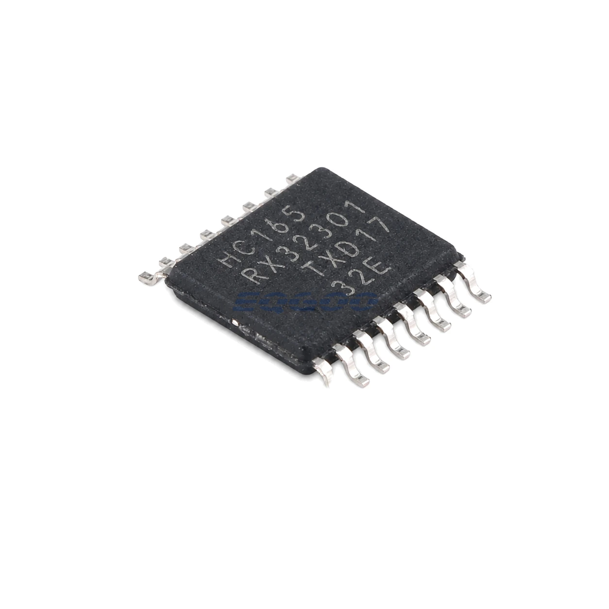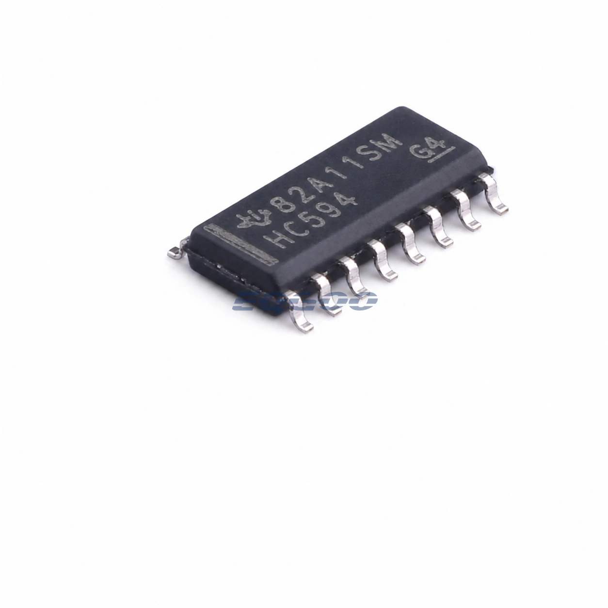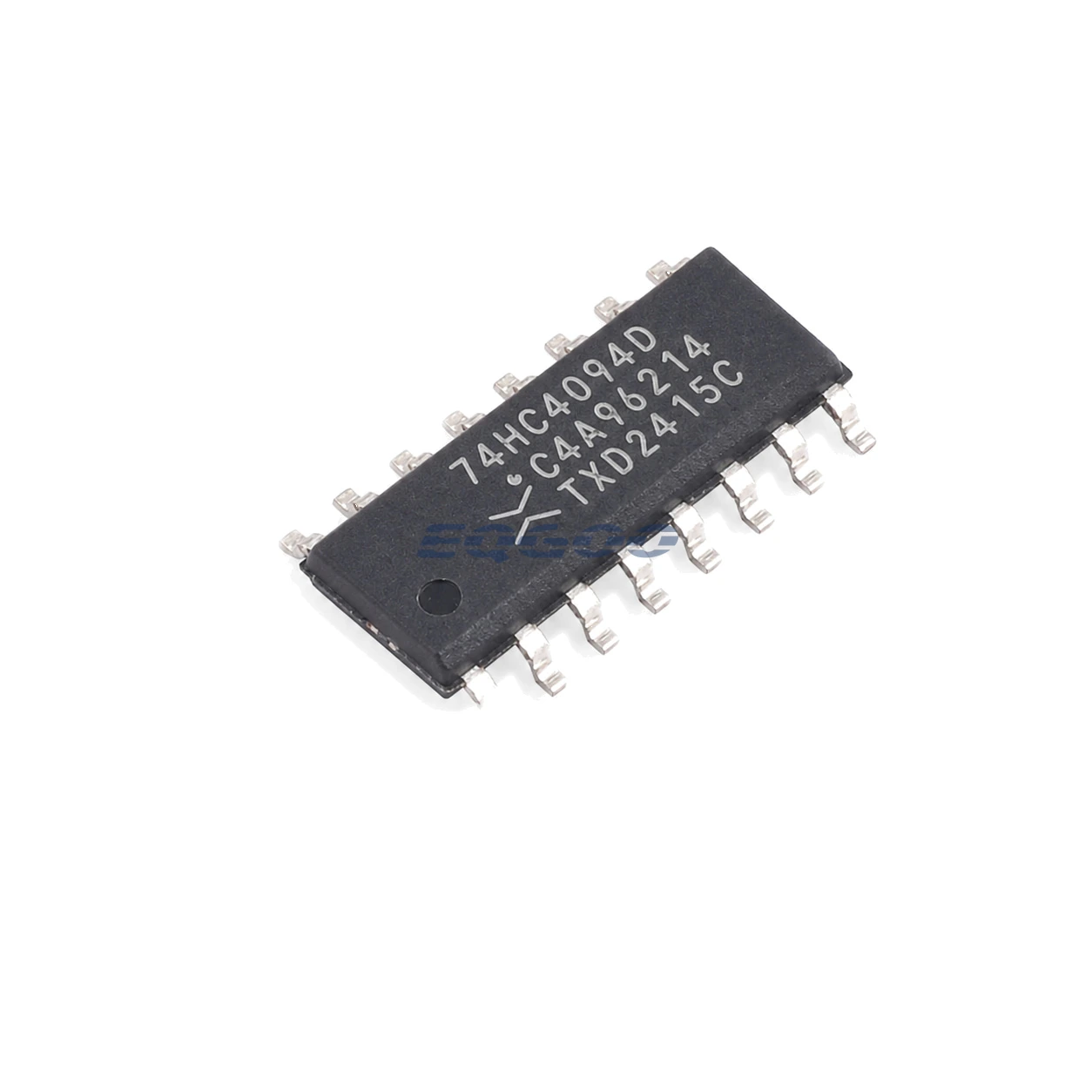
Device Overview
Designed as a 8-stage shift-and-store bus register, Nexperia 74HC4094D,653 uses the SOIC-16 package. The main engineering checks for this variant are Device Function (8-stage shift-and-store bus register), Supply Voltage (2.0 to 6.0 V), Bit Count (8).
Selection-Critical Data
| Parameter | Confirmed Data | Why It Matters |
|---|---|---|
| Device Function | 8-stage shift-and-store bus register | Defines the device function or architecture that a compatible replacement must preserve before secondary ratings are compared. |
| Supply Voltage | 2.0 to 6.0 V | Defines compatibility with the available board power rail and required bias range. |
| Bit Count | 8 | Defines the parallel state/register width and therefore how many bits can be stored, shifted or controlled per device. |
| Maximum Frequency | 95 MHz (74HC4094 D/PW parametric) | Defines the operating frequency or RF band that must cover the intended signal frequencies. |
| Output Drive | ±5.2 mA (parametric class) | Defines output drive strength and therefore the external load, fanout or pull-up/down burden the pin can support. |
| Exact Package | SOIC-16 | Determines PCB footprint, pinout, mechanical assembly and orderable-variant compatibility. |
Logic and Interface Selection Notes
At 8-stage shift-and-store bus register, the device function defines the device function or architecture that a compatible replacement must preserve before secondary ratings are compared.
For supply voltage, 2.0 to 6.0 V is the approved value. Defines compatibility with the available board power rail and required bias range. The maximum frequency is 95 MHz; this defines the operating frequency or RF band that must cover the intended signal frequencies. Technical condition: 74HC4094 D/PW parametric.
Exact Package is SOIC-16. Determines PCB footprint, pinout, mechanical assembly and orderable-variant compatibility.
For bit count, 8 is the approved value. Defines the parallel state/register width and therefore how many bits can be stored, shifted or controlled per device. For output drive, +/-5.2 mA is the approved value. Defines output drive strength and therefore the external load, fanout or pull-up/down burden the pin can support. Technical condition: parametric class.
For the same Nexperia 74HC4094 8-stage shift-and-store register in a smaller PCB footprint, compare 74HC4094PW,118 in 16-pin TSSOP with this 74HC4094D,653 in 16-pin SOIC. The logic family is shared, but the SOT403-1 and SOT109-1 package outlines and PCB land patterns differ; verify your board footprint before selecting the other order code.