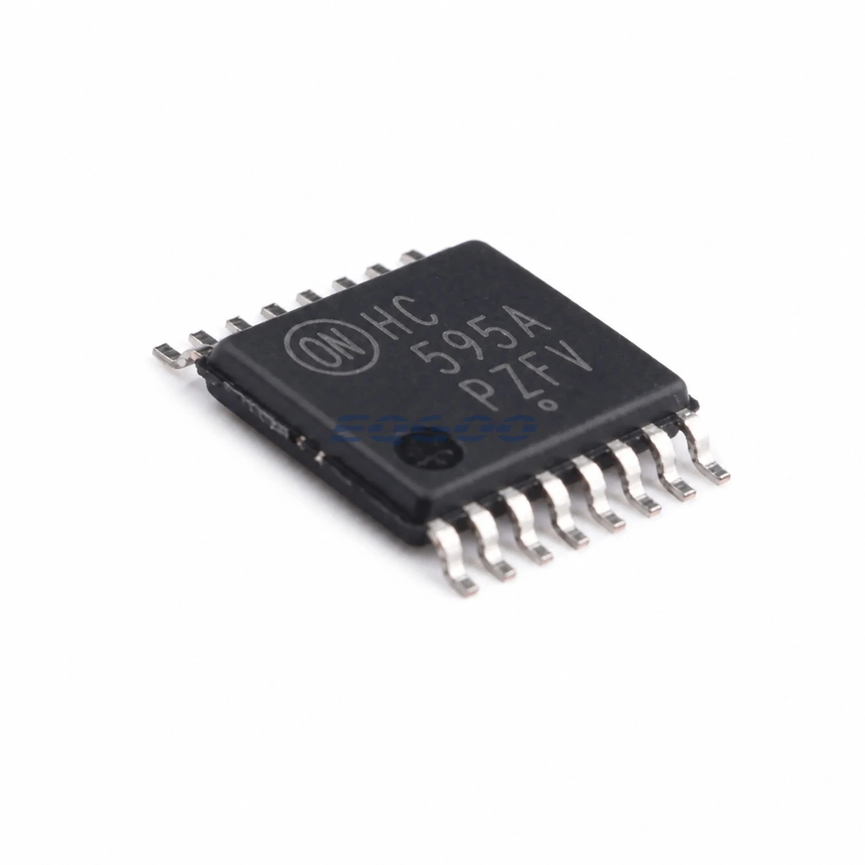
Device Overview
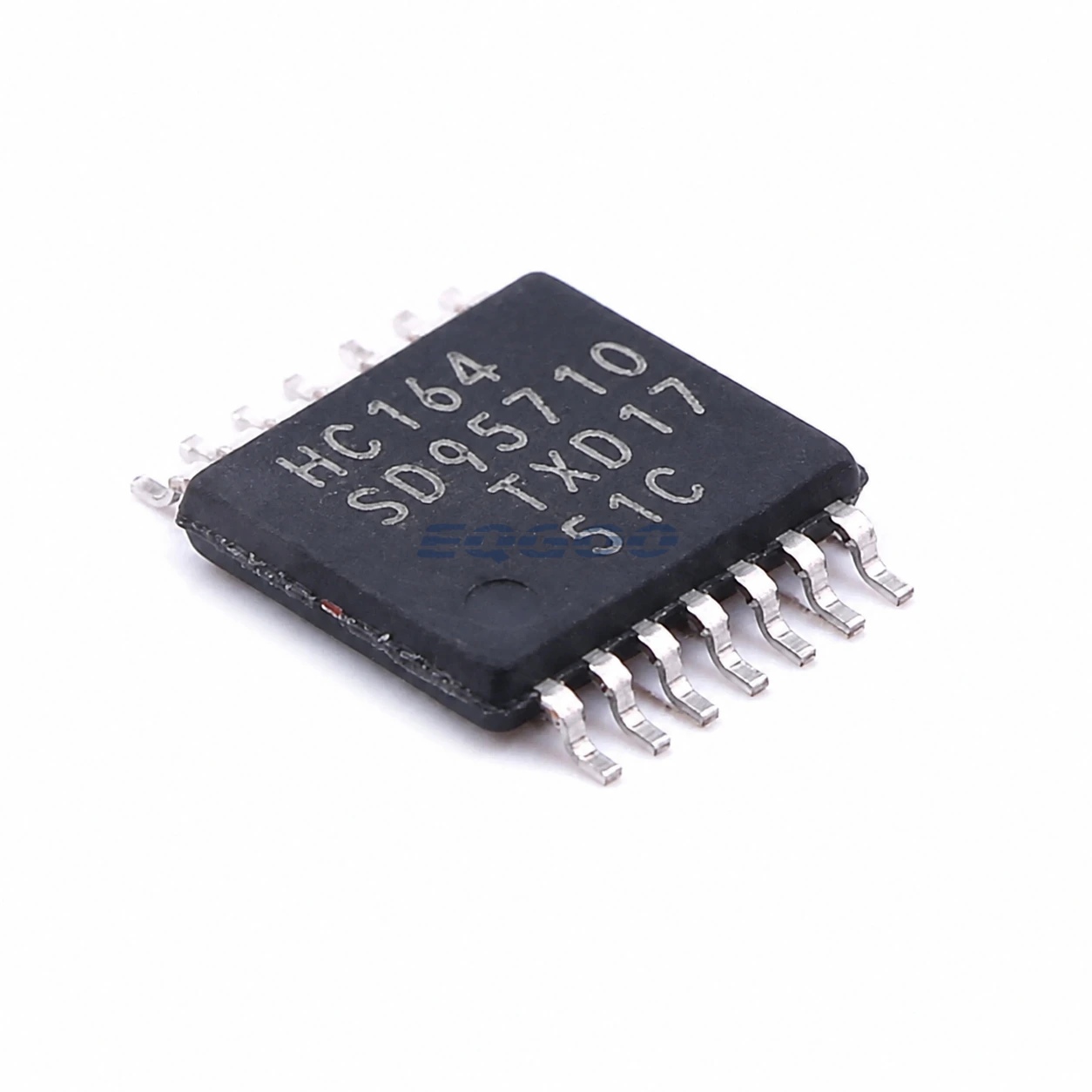
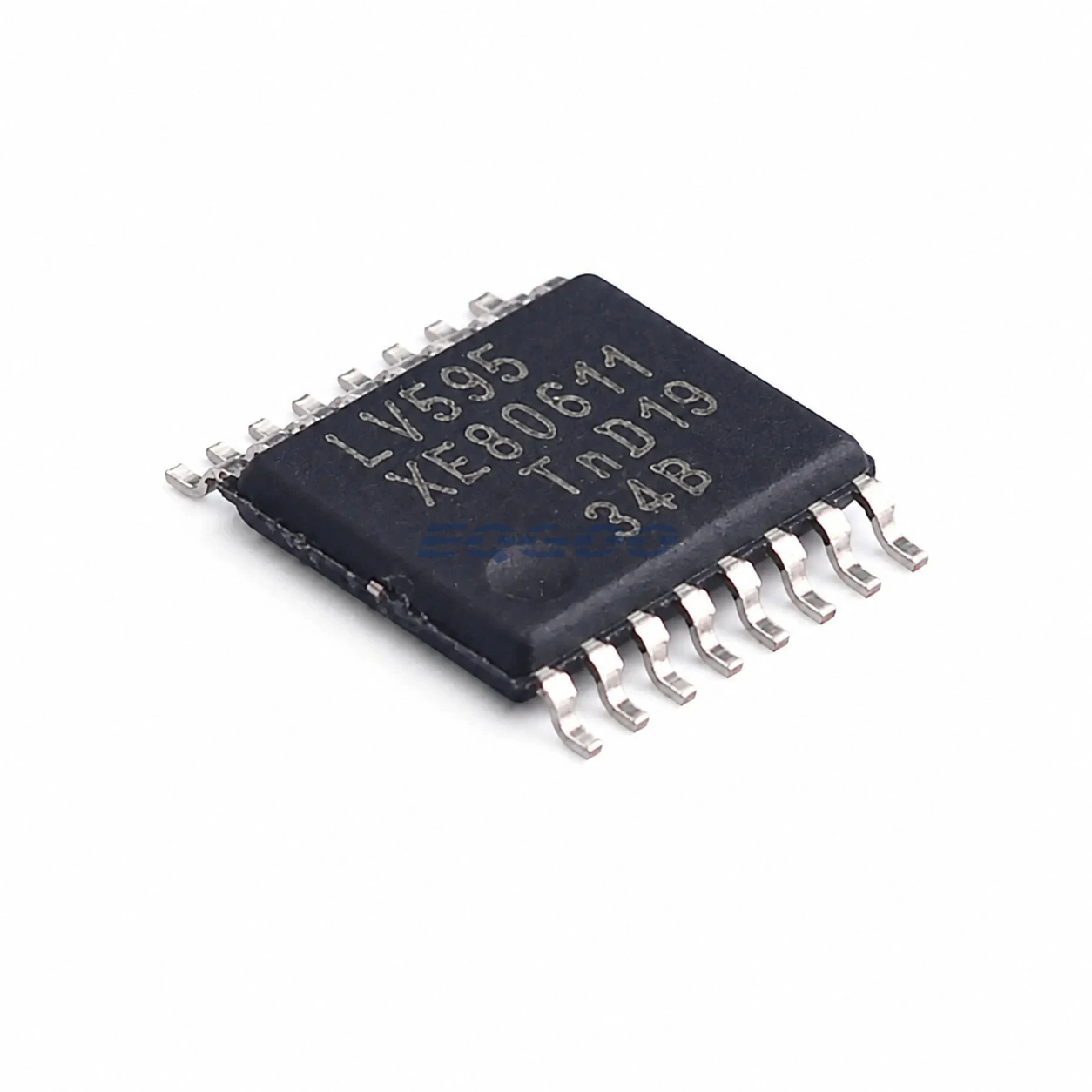
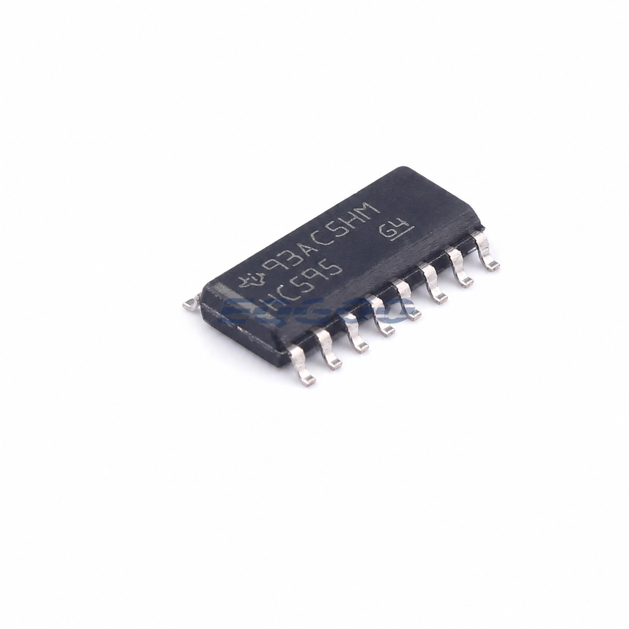
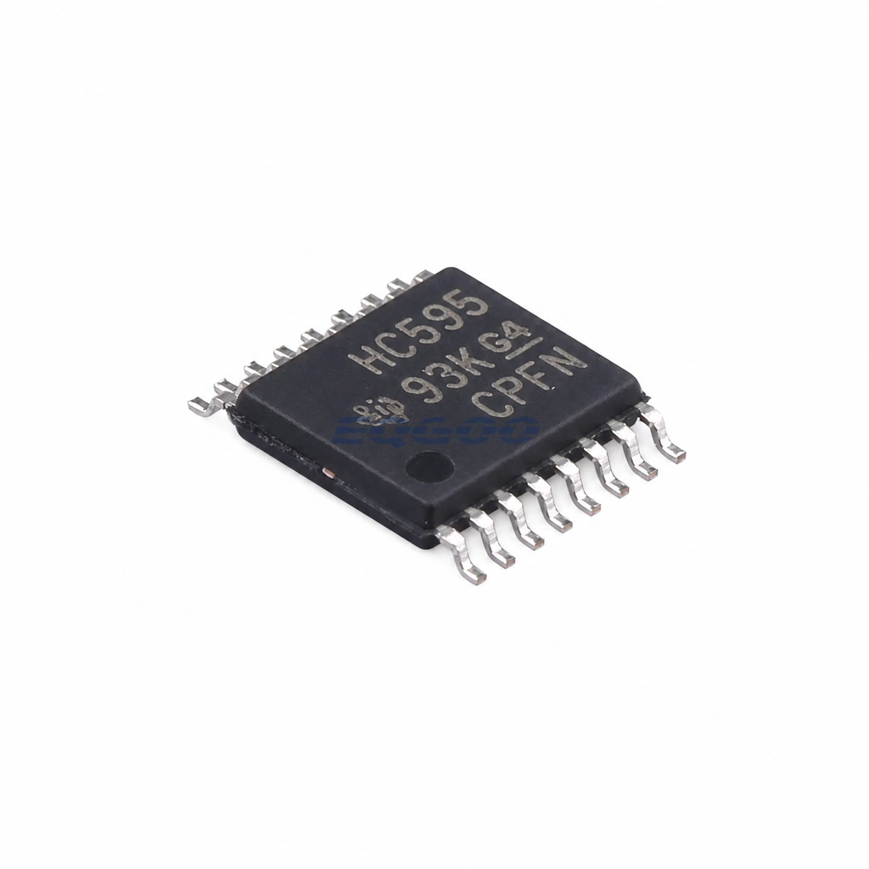
MC74HC595ADTR2G is the TSSOP-16 tape-and-reel version of onsemi’s MC74HC595A 8-bit serial-input shift register. The device combines an 8-bit shift register with a separate 8-bit D-type storage latch, so serial data can be shifted in before all eight parallel outputs are updated together. The parallel outputs can also be placed in a high-impedance state through the independent output-enable input.
The HC device operates from 2.0 V to 6.0 V. Its serial input and clock structure can interface directly with SPI-style serial ports on CMOS processors, while the serial SQH output allows multiple devices to be cascaded for wider output expansion.
Confirmed Technical and Ordering Data
| Parameter | Confirmed value | Scope / condition |
|---|---|---|
| Device Function | 8-bit serial-input shift register with 8-bit D-type storage latch and 3-state parallel outputs | Manufacturer documented |
| Protocol Or Logic Function | Standard CMOS serial-to-parallel shift-register logic; directly interfaces SPI serial data ports | Manufacturer documented |
| Channels | 8 parallel latched outputs | Manufacturer documented |
| Supply Voltage | 2.0 to 6.0 V | HC device |
| Data Rate | 4 MHz at 2.0 V; 8 MHz at 3.0 V; 20 MHz at 4.5 V; 24 MHz at 6.0 V | guaranteed maximum clock frequency; limits for temperatures up to 125 °C; higher values apply at lower temperature |
| Direction Topology | Serial data input A; serial output SQH; latched parallel outputs QA-QH | Manufacturer documented |
| Output Control | Asynchronous shift-register reset and independent output enable for 3-state parallel outputs | Manufacturer documented |
| Drive Capability | 15 LSTTL loads | output drive capability |
| Io Levels | HC inputs are Standard CMOS compatible; TTL interfacing can use pull-up resistors | Manufacturer documented |
| Exact Package | TSSOP-16 DT suffix; 2500 units / Tape & Reel | Manufacturer documented |
| Temperature Grade | -55 to 125 °C | datasheet guaranteed-characteristic temperature span |
Engineering Selection Guidance
Clock capability depends strongly on supply voltage and temperature. For the guaranteed limits through 125 °C, the datasheet gives maximum clock frequencies of 4 MHz at 2.0 V, 8 MHz at 3.0 V, 20 MHz at 4.5 V and 24 MHz at 6.0 V. Those values should remain tied to their VCC conditions rather than being reduced to one unconditional speed rating.
The shift clock and latch clock are independent. That separation is useful when output glitches must be avoided: new serial data can be loaded into the shift register while the existing QA-QH state remains latched, then transferred to all parallel outputs with the latch clock.
Asynchronous reset clears the shift register, while output enable controls only the three-state parallel outputs. These are different control functions and should not be treated as interchangeable reset paths. The exact ADTR2G orderable uses the 16-pin TSSOP package and tape-and-reel shipping format.
Lifecycle and Procurement
onsemi currently lists MC74HC595ADTR2G in its active product/orderable set. The exact package is TSSOP-16 and the documented operating temperature span used for this page is -55 to 125 °C. Manufacturer lifecycle status does not state HKEQGOO stock, lead time, MOQ or final availability.
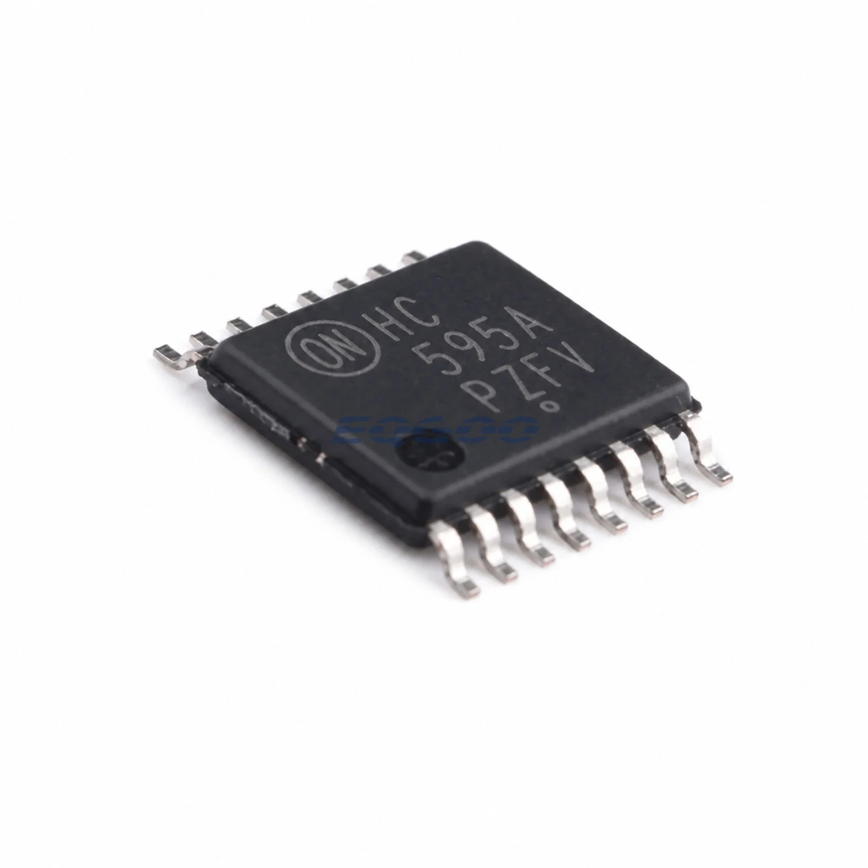
Official Engineering Resources
Quality & Verification Support
Third-party inspection or testing can be arranged according to customer requirements. Testing fees are borne by the buyer. Additional verification requirements can be discussed before shipment.
Request a Quote
For MC74HC595ADTR2G sourcing, provide the required quantity, destination, target Date Code if applicable, and any inspection or testing requirements.