Device Overview
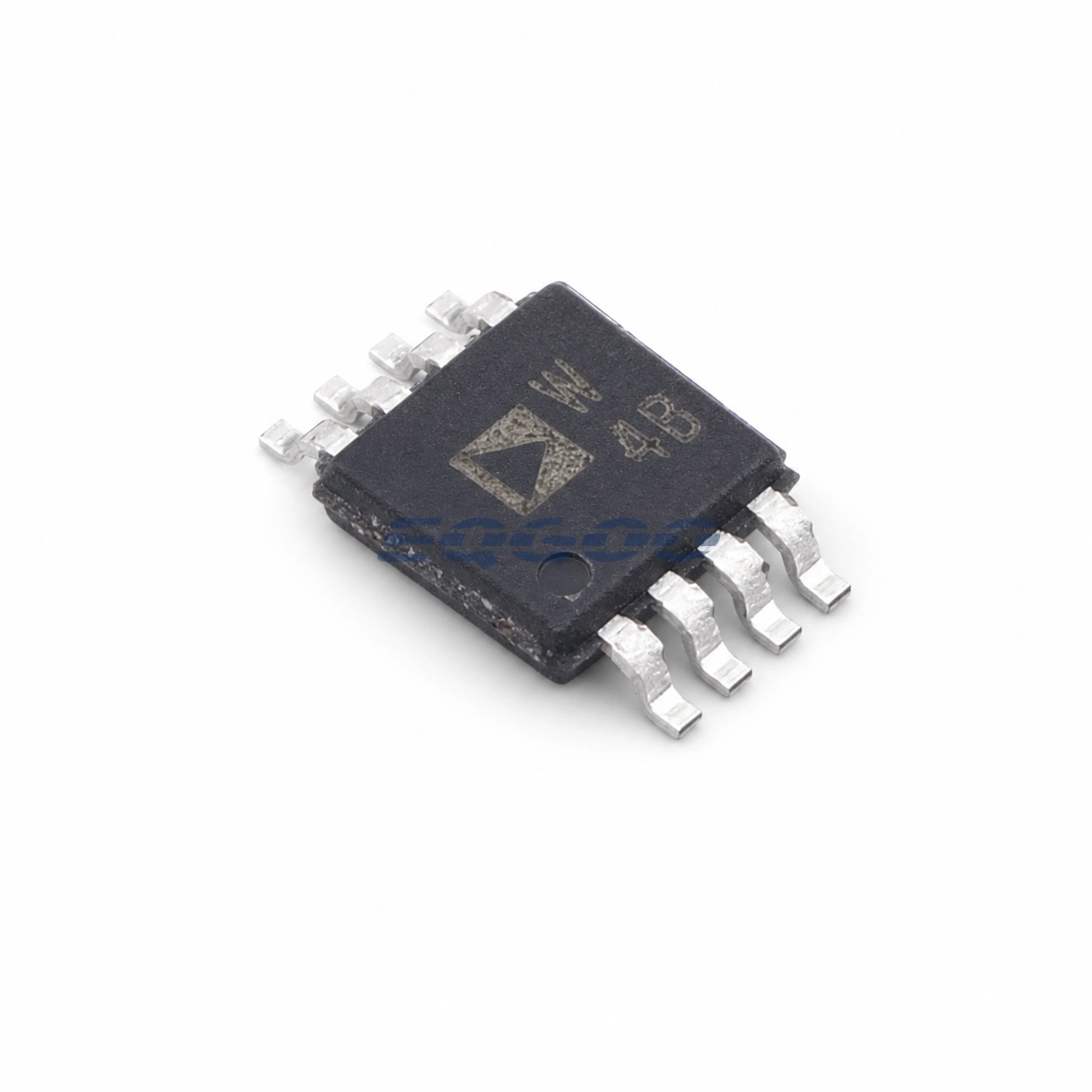
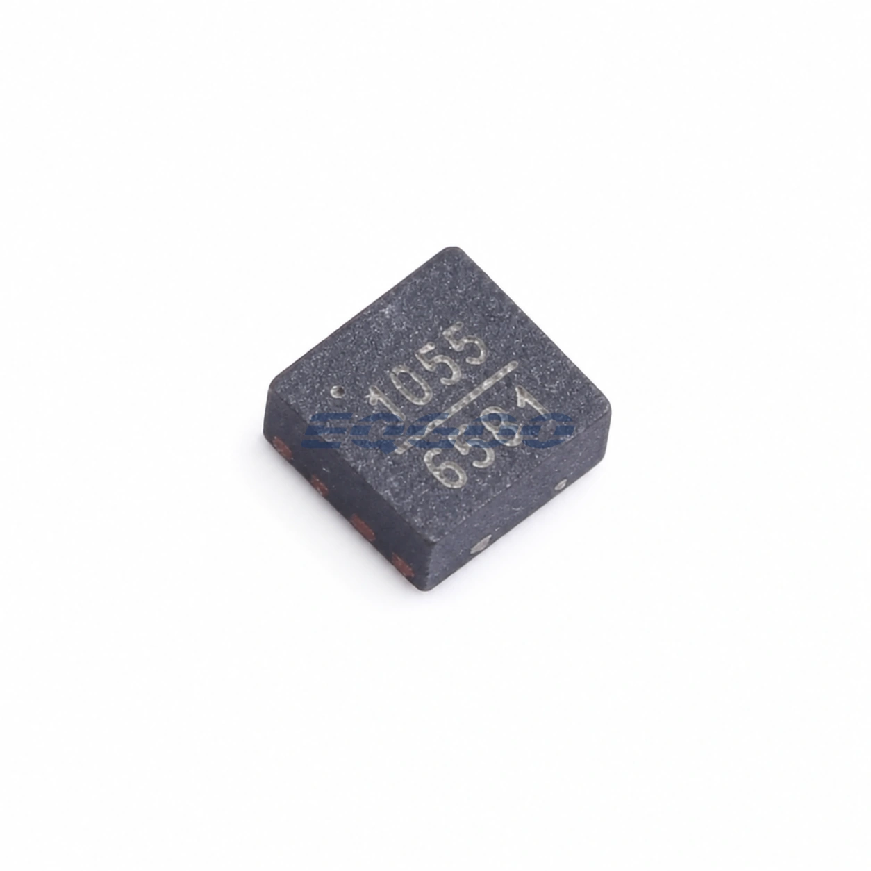
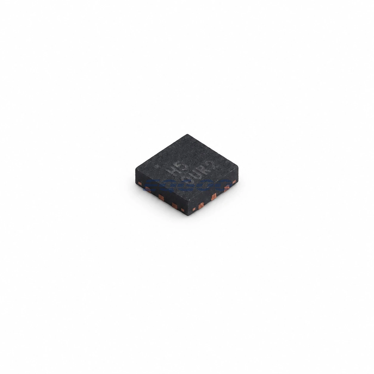
RFSW8006QTR7 is a Qorvo SP3T SOI in a DFN-8 package. The main engineering checks for this variant are Switch Topology (SP3T SOI), Frequency Range (100 to 4000 MHz), Insertion Loss (0.6 dB).
Selection-Critical Data
| Parameter | Confirmed Data | Why It Matters |
|---|---|---|
| Switch Topology | SP3T SOI (Exact manufacturer datasheet) | Defines the RF port-routing topology (for example SP3T) that must match the required signal-path switching function. |
| Frequency Range | 100 to 4000 MHz | Defines the operating frequency or RF band that must cover the intended signal frequencies. |
| Insertion Loss | 0.6 dB (2.4 GHz typical) | Defines signal loss through the RF path and therefore contributes directly to the link budget. |
| Isolation | 27 dB (2.4 GHz headline value; path-specific values vary) | Defines suppression of unwanted coupling between RF paths or switch states at the stated frequency. |
| Compression | 27 dBm at 3.6 V headline P0.1dB (Manufacturer features) | Defines output compression headroom and must be compared at matching frequency and bias conditions. |
| Supply Voltage | 2.7 to 4.8 V | Defines compatibility with the available board power rail and required bias range. |
| Control Voltage | 1.2 to 4.8 V (High-state control) | Defines the electrical voltage envelope that must cover the intended operating or stress level. |
| Exact Package | 8-pin DFN, 2.0 x 2.0 x 0.85 mm (Exact orderable evidence) | Determines PCB footprint, pinout, mechanical assembly and orderable-variant compatibility. |
| Rf Function | RF switch | Defines the device function or architecture that a compatible replacement must preserve before secondary ratings are compared. |
| Lifecycle / Procurement | Production | Supports current sourcing and new-design consideration. |
RF Selection Notes
100 to 4000 MHz is the stated frequency range value. Defines the operating frequency or RF band that must cover the intended signal frequencies. At RF switch, the rf function defines the device function or architecture that a compatible replacement must preserve before secondary ratings are compared.
At 0.6 dB, the insertion loss defines signal loss through the RF path and therefore contributes directly to the link budget. Technical condition: 2.4 GHz typical. For isolation, 27 dB is the approved value. Defines suppression of unwanted coupling between RF paths or switch states at the stated frequency. Technical condition: 2.4 GHz headline value; path-specific values vary.
For compression, 27 dBm at 3.6 V headline P0.1dB is the approved value. Defines output compression headroom and must be compared at matching frequency and bias conditions. Technical condition: Manufacturer features.
The supply voltage is 2.7 to 4.8 V; this defines compatibility with the available board power rail and required bias range.
8-pin DFN, 2.0 x 2.0 x 0.85 mm is the stated exact package value. Determines PCB footprint, pinout, mechanical assembly and orderable-variant compatibility. Technical condition: Exact orderable evidence.
At SP3T SOI, the switch topology defines the RF port-routing topology (for example SP3T) that must match the required signal-path switching function. Technical condition: Exact manufacturer datasheet. Control Voltage is 1.2 to 4.8 V. Defines the electrical voltage envelope that must cover the intended operating or stress level. Technical condition: High-state control.