Device Overview
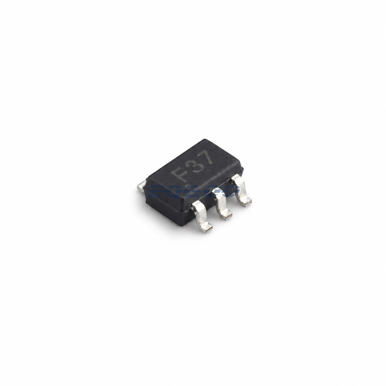
Qorvo SZA-3044Z is an exact-order RF amplifier supplied in 20-pin QFN, 4 x 4 mm. Selection of this exact part is driven primarily by Frequency Range (2.7 GHz to 3.8 GHz), Gain (26.0 dB), Noise Figure (5.0 dB).
Selection-Critical Data
| Parameter | Confirmed Data | Why It Matters |
|---|---|---|
| Frequency Range | 2.7 GHz to 3.8 GHz | Defines the operating frequency or RF band that must cover the intended signal frequencies. |
| Gain | 26.0 dB | Sets the signal-level gain budget and must be compared at matching frequency, mode and bias conditions. |
| Noise Figure | 5.0 dB | Defines the device contribution to receiver noise and must be compared at matching frequency and bias conditions. |
| P1dB | 31 dBm | Defines output compression headroom and must be compared at matching frequency and bias conditions. |
| Output Power | 24.0 dBm | Defines available output-power headroom under the stated operating conditions; compare it at the same frequency, modulation/load and bias. |
| Exact Package | 20-pin QFN, 4 x 4 mm | Determines PCB footprint, pinout, mechanical assembly and orderable-variant compatibility. |
| Rf Function | RF amplifier | Defines the device function or architecture that a compatible replacement must preserve before secondary ratings are compared. |
| Power Added Efficiency | 14.5 % | Defines a selection-critical engineering characteristic that a compatible substitute must preserve under the stated conditions. |
| Supply Voltage | 3 / 6 V (Min / Max) | Defines compatibility with the available board power rail and required bias range. |
| Impedance | 50 Ohm | Defines RF matching compatibility with the surrounding transmission-line and matching network. |
RF Selection Notes
Frequency Range is 2.7 GHz to 3.8 GHz. Defines the operating frequency or RF band that must cover the intended signal frequencies. RF amplifier is the stated rf function value. Defines the device function or architecture that a compatible replacement must preserve before secondary ratings are compared.
At 26.0 dB, the gain sets the signal-level gain budget and must be compared at matching frequency, mode and bias conditions. Noise Figure is 5.0 dB. Defines the device contribution to receiver noise and must be compared at matching frequency and bias conditions.
At 31 dBm, the p1db defines output compression headroom and must be compared at matching frequency and bias conditions. 24.0 dBm is the stated output power value. Defines available output-power headroom under the stated operating conditions; compare it at the same frequency, modulation/load and bias.
For supply voltage, 3 / 6 V is the approved value. Defines compatibility with the available board power rail and required bias range. Technical condition: Min / Max. For impedance, 50 Ohm is the approved value. Defines RF matching compatibility with the surrounding transmission-line and matching network.
For exact package, 20-pin QFN, 4 x 4 mm is the approved value. Determines PCB footprint, pinout, mechanical assembly and orderable-variant compatibility.
Power Added Efficiency is 14.5 %. Defines a selection-critical engineering characteristic that a compatible substitute must preserve under the stated conditions.