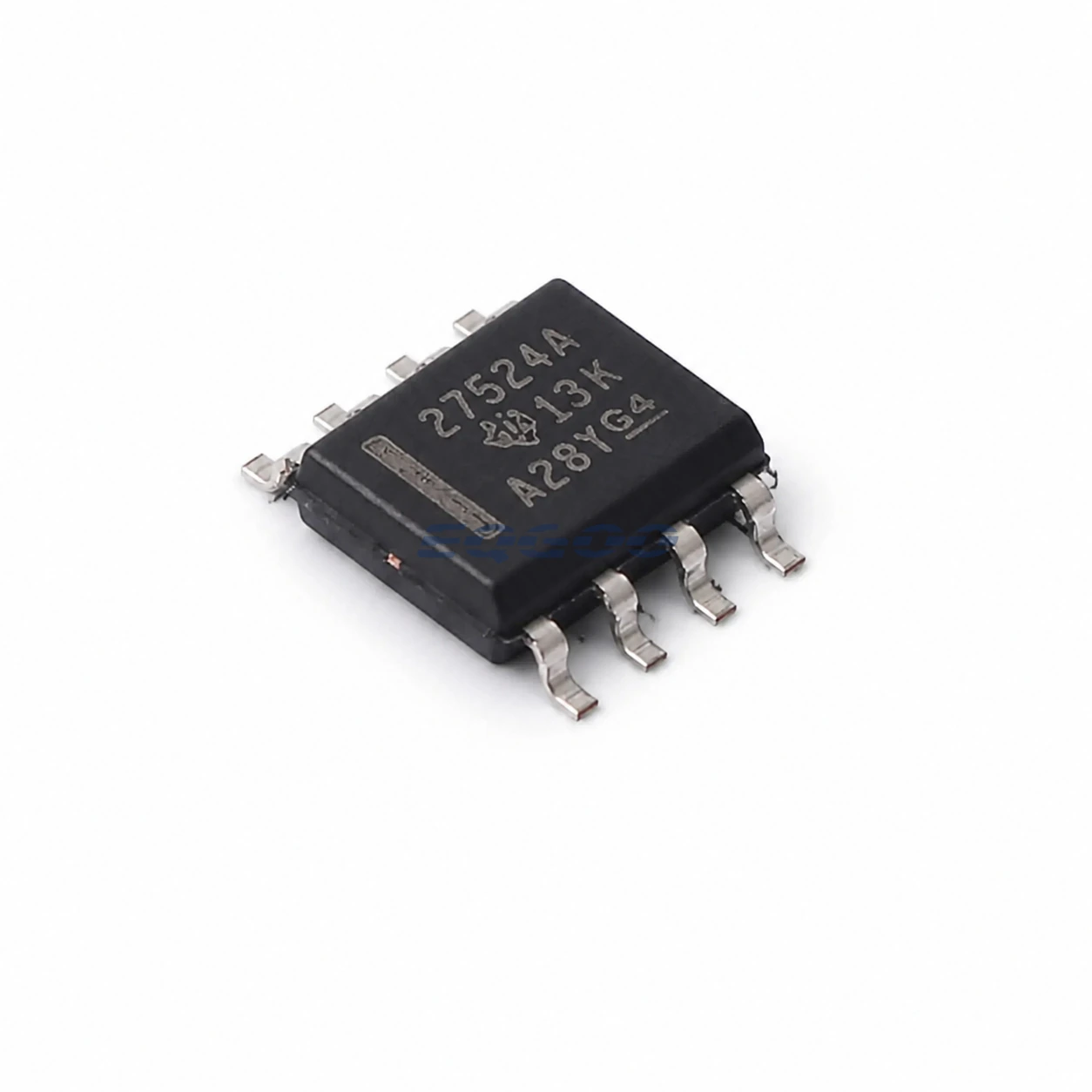

Key Selection Information
| Selection Parameter | Confirmed Information |
|---|---|
| Channels | 2 independent non-inverting low-side drivers |
| Peak Drive | 5 A source / 5 A sink each |
| Supply | 4.5 V to 18 V |
| Input Robustness | Inputs tolerate −5 V stated feature |
| Control | Independent enable per channel |
| Timing | 17 ns typical delay; ~1 ns typical channel matching |
| Temperature | −40°C to +150°C junction stated family range |
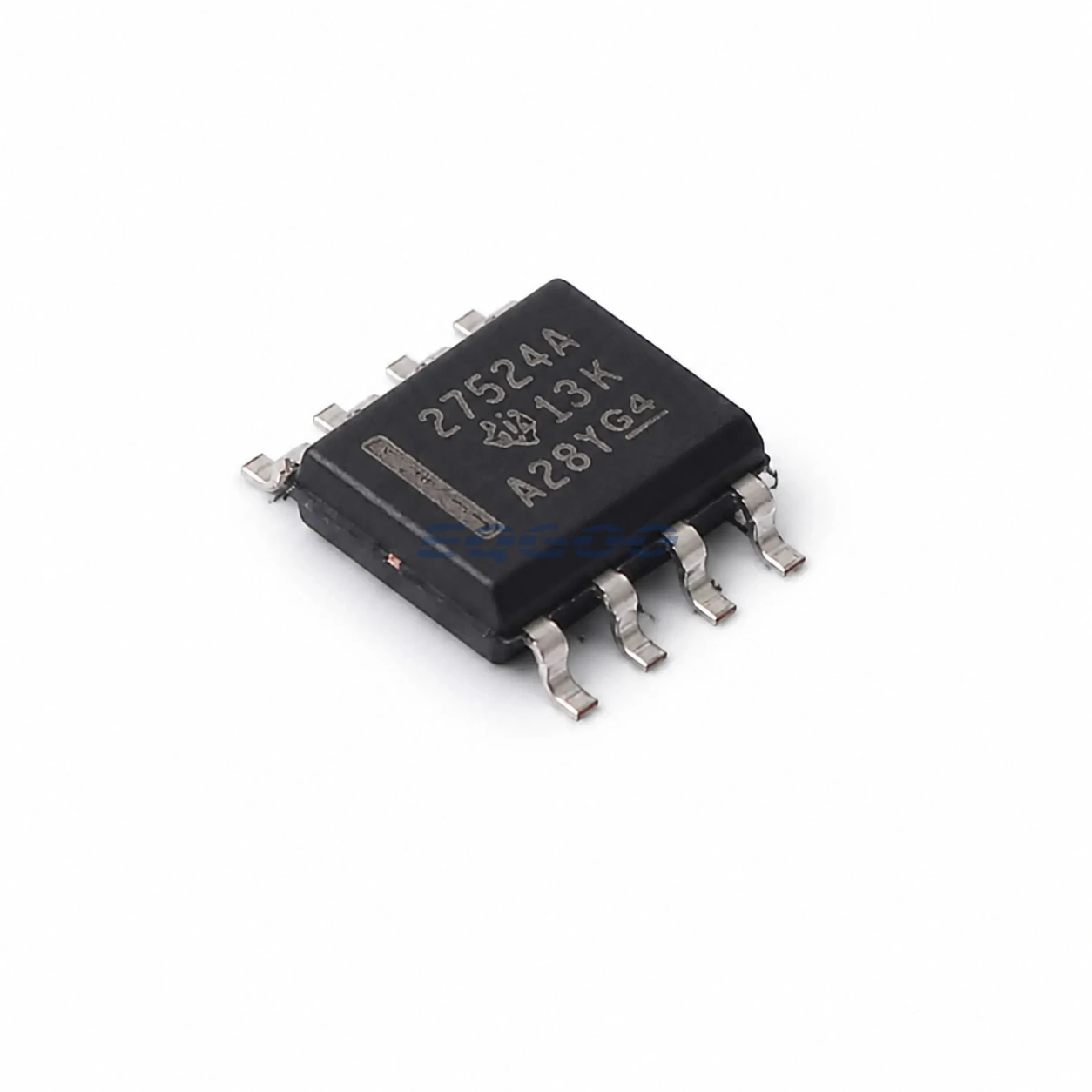
| Exact Package / Packing | SOIC (D), 8 pins; large tape and reel |
Product Overview
UCC27524ADR integrates two 5 A low-side gate drivers with closely matched delay, reducing component count in dual-switch power stages. The A variant adds direct input tolerance to −5 V, useful in noisy layouts where PWM control lines can undershoot ground.
Independent enables let each gate channel be inhibited separately, while the two outputs can also be paralleled when one larger gate requires additional current. Delay matching becomes important when the channels drive related power paths.
The DR exact order code uses conventional SOIC-8, favoring visible leads and easy probing in power-supply development/production.
For related devices, see HKEQGOO’s Gate Drivers category.
Technical Specifications
| Parameter | Verified Information |
|---|---|
| Manufacturer | Texas Instruments |
| Exact MPN | UCC27524ADR |
| Channels | 2 independent non-inverting low-side drivers |
| Peak Drive | 5 A source / 5 A sink each |
| Supply | 4.5 V to 18 V |
| Input Robustness | Inputs tolerate −5 V stated feature |
| Control | Independent enable per channel |
| Timing | 17 ns typical delay; ~1 ns typical channel matching |
| Temperature | −40°C to +150°C junction stated family range |
| Exact Package / Packing | SOIC (D), 8 pins; large tape and reel |
| Manufacturer Status | Active / Production |
| Part Marking | 27524A |
Functional Highlights
Negative input tolerance improves noise/transient robustness
Fast power edges can capacitively or inductively drive controller traces below ground. The −5 V input capability gives more margin than relying on external clamp current alone.
Matched dual channels reduce timing spread
About 1 ns typical delay matching is useful in interleaved or paired paths, although system skew also includes PWM source, trace and gate-network mismatch.
Design Considerations
- Do not treat input −5 V tolerance as permission for sustained large negative current outside the stated conditions.
- If paralleling outputs, route both channels symmetrically to avoid current imbalance/ringing.
- Use separate local gate resistors when each channel drives a different switch.
Product Status and Exact Order Code
Manufacturer status: Active / Production
Texas Instruments lists UCC27524ADR as Active / Production; SOIC (D), 8 pins; large tape-and-reel option; −40°C to +140°C orderable range; marking 27524A.
Related Engineering Resources
Quality & Verification Support
Third-party inspection or testing can be arranged according to customer requirements. Testing fees are borne by the buyer. Additional verification requirements can be discussed before shipment. After an order is placed, physical product, label, packaging, and Date Code photos may be provided where appropriate.
Request a Quote
To request a quotation, provide the manufacturer part number, required quantity, destination, target Date Code if applicable, and any testing or inspection requirements.