Key Selection Information
| Selection Parameter | Confirmed Information |
|---|---|
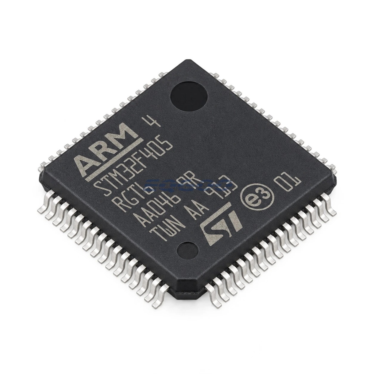
| Package | LQFP-64(10×10) |
| Supply voltage | 1.71V~3.6V |
| CPU Core | Arm Cortex-M4 with FPU |
| Maximum CPU speed | 170MHz |
| Program memory | 512KB |
| Operating Temperature | -40℃~+85℃ |
| Number of I/O | 52 |
Mixed-signal STM32G4 with control-focused hardware
STM32G474RET6 combines a 170 MHz Arm Cortex-M4 core with FPU/DSP, 512 KB of Flash and an industrial LQFP-64 package. ST’s exact-orderable data lists 52 I/Os for this device.
The part is differentiated by the STM32G4 control and analog subsystem rather than CPU frequency alone: ST lists six integrated op amps, seven comparators, seven 12-bit DAC channels and three FDCAN controllers for the exact orderable, while the family also includes mathematical accelerators and high-resolution timing resources. These blocks can reduce the amount of external analog/control support needed around the MCU when they match the design’s signal chain.
Technical Specifications
| Parameter | Value |
|---|---|
| Package | LQFP-64(10×10) |
| Supply voltage | 1.71V~3.6V |
| CPU Core | Arm Cortex-M4 with FPU |
| Maximum CPU speed | 170MHz |
| Program memory | 512KB |
| Operating Temperature | -40℃~+85℃ |
| Number of I/O | 52 |
| DAC (Bit) | 12bit |
| ADC (Bit) | 12bit |
| Program Memory Type | FLASH |
| Core Size | 32 Bit |
| Oscillator Type | Built-in |
Why the RE / T6 combination matters
The RE density fixes 512 KB of program Flash while T6 identifies the industrial LQFP-64 orderable. That package exposes 52 I/Os, so the practical selection question is whether the required analog channels, PWM/timer outputs, FDCAN and serial interfaces all fit the 64-pin pin map at the same time.
Prioritize the analog and control resource map
- Analog integration: six op amps and seven comparators make front-end partitioning a real selection axis, but each function must be checked against the exact pin map.
- Timing: high-resolution timing and the STM32G4 timer architecture are useful where control-loop timing is more important than simply maximizing general-purpose GPIO.
- Communications: three FDCAN controllers are integrated; each physical CAN bus still needs an external transceiver.
- Memory: 512 KB Flash should be budgeted against control firmware, communication stacks and update margin before the PCB is frozen.
Best-fit system profile
This configuration is strongest when the design benefits from tight coupling between computation, analog signal conditioning, high-resolution timing and CAN FD communication. If the application does not need that integrated analog/control feature set, a simpler MCU may provide the required CPU and memory with less peripheral overhead.
Integration checks for the 64-pin orderable
Verify the LQFP-64 alternate-function map before committing ADC, DAC, op-amp, comparator, timer and FDCAN signals, because the headline peripheral count does not imply every function can be used simultaneously. Keep the 1.71 V to 3.6 V supply range and analog-reference strategy visible during power-tree and PCB planning, and add external CAN transceivers for any FDCAN buses.
Related Engineering Resources
- STM32G474RET6 Datasheet (PDF) — HKEQGOO-hosted technical copy for engineering review.
- STMicroelectronics product page — official manufacturer product, lifecycle and ordering resource.
Quality & Verification Support
Third-party inspection or testing can be arranged according to customer requirements. Testing fees are borne by the buyer. Additional verification requirements can be discussed before shipment. After an order is placed, physical product, label, packaging, and Date Code photos may be provided where appropriate.
Request a Quote
To request a quotation, provide the manufacturer part number, required quantity, destination, target Date Code if applicable, and any testing or inspection requirements.