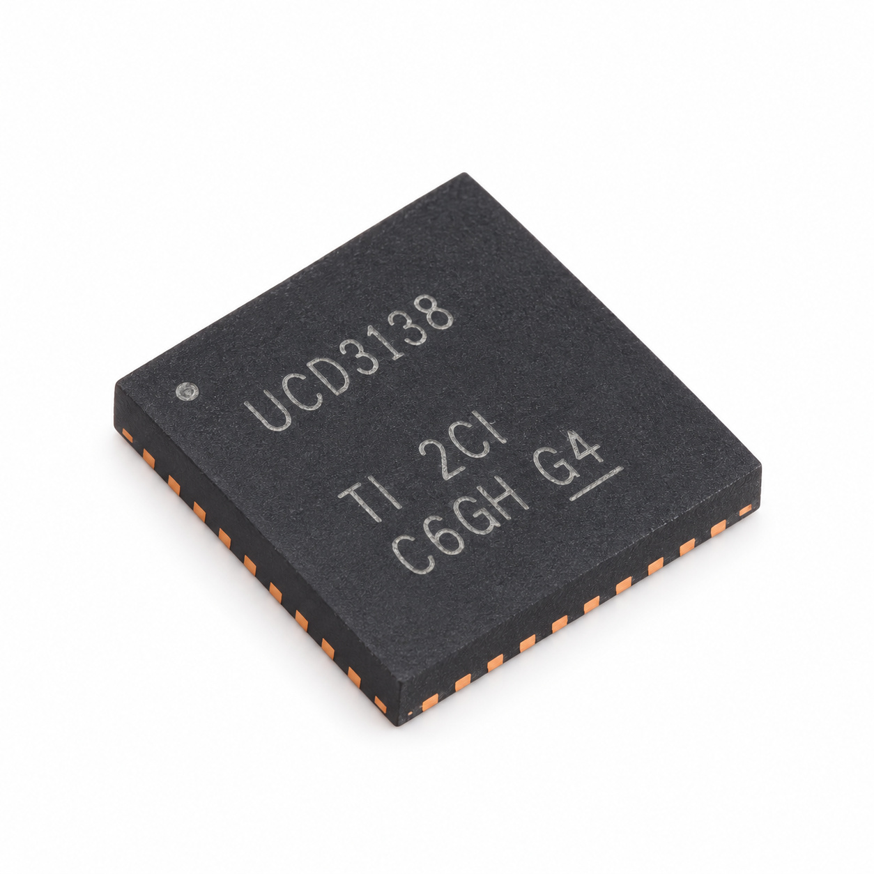
The Texas Instruments UCD3138RHAR is a digitally programmable controller for isolated power supplies, offered as an RHA 40-pin VQFN, 6 × 6 mm exposed-pad package. It supplies digital feedback processing and DPWM control signals to an external power stage; it is not a self-contained 1 A, 3 A or fixed-voltage regulator. The exact RHAR orderable has a manufacturer 2,500-piece large tape-and-reel configuration, which should not be confused with customer MOQ or inventory.
Exact UCD3138RHAR electrical and resource data
| Feature | Exact specification | Selection qualifier |
|---|---|---|
| Architecture | Programmable isolated-power digital controller | 32-bit ARM7TDMI-S processor, not an integrated isolated power module |
| Processor clock | 31.25 MHz | Master clock; not the DPWM output-switching frequency |
| Independent feedback loops | 3 | TI’s RHA 40-pin resource matrix, rather than maximum count across all family packages |
| DPWM outputs | 8 | Exact 40-pin RHA resources, subject to peripheral and pin mux configuration |
| DPWM pulse-width resolution | 250 ps | Pulse-width step size, distinct from frequency and phase resolution |
| DPWM frequency/phase resolution | 4 ns | Separate timing parameter |
| DPWM switching capability | Up to 2 MHz | Configurable controller capability, not guaranteed converter switching in every power stage |
| ADC12 inputs | 7 channels, 12-bit | Exact RHA 40-pin matrix; general-purpose conversion sampling rate 267 ksps |
| EADC | 16 MHz sampling | Configurable error ADC with manufacturer feature resolution as fine as 1 mV/LSB |
| Program Flash | 32 KB | Exact 40-pin configuration, not another package’s advertised maximum |
| Data Flash / Data RAM | 2 KB ECC Data Flash / 4 KB RAM | Distinct nonvolatile and volatile resources; Data Flash is not EEPROM |
| Boot ROM | 4 KB | Part of device boot and firmware-management architecture |
| UART interfaces | 1 | Exact 40-pin device matrix |
| GPIO resources | 18 | Pin-multiplexed; not all interface functions can necessarily be exposed simultaneously |
| Analog comparators | 6 | Exact RHA 40-pin resource matrix |
| I²C/PMBus timing | 100–1,000 kHz | TI timing scope for this orderable family; check firmware and bus-mode configuration |
| Recommended V33D supply | 3.0–3.6 V | Digital operating rail; +3.8 V is absolute maximum, not recommended operation |
| Recommended V33A supply | 3.0–3.6 V | Analog rail requires its own suitable filtering and returns |
| V33DIO on 40-pin package | Internally connected to V33D | Do not assume a separate independently adjustable 40-pin I/O supply |
| Recommended BP18 | 1.6–2.0 V | BP18 supply range; +2.5 V is absolute-maximum stress |
| Operating junction temperature | −40 to +125 °C | TJ qualification, not an ambient temperature guarantee |
| RHA package thermal resistance | 31.8 °C/W RθJA | Package thermal metric under specified reference conditions, not every PCB result |
| Analog supply test current | 6.3 mA | V33A powered with general ADC/EADC sampling disabled |
| Digital ROM-execution current | 60 mA | V33D measured during ROM execution |
| Digital flash-programming current | 70 mA | V33D while Flash programming in ROM mode |
| Total current test | 100 mA | TI ROM-mode, all DPWM channels at 2 MHz and unloaded |
| Original manufacturer’s pack | RHA VQFN-40, 6 × 6 mm, 2,500 large-reel units | Full ordering code UCD3138RHAR; not proof of present stock |
Why the RHA suffix matters to engineers and buyers
The RHA VQFN-40 package has its own pin mapping, exposed pad and footprint requirements. The RHAR suffix should not be interchanged with UCD3138ARMHR, which is a UCD3138A-family RMH WQFN-40 orderable, merely because both use 40 pins and 6 × 6 mm bodies. Before replacing a controller, verify pin assignments, peripheral mux, firmware compatibility, electrical grade, land pattern and any quality requirements from original manufacturer documentation.
On this RHA 40-pin device, TI’s resource matrix gives 3 independent loops, 8 DPWM outputs, 7 ADC12 channels, 1 UART, 18 GPIO and 32 KB program Flash. Using broader family-level counts would overstate what an exact RHAR design exposes. The 250 ps DPWM pulse-width resolution and 4 ns frequency/phase resolution are distinct controls; neither by itself establishes efficiency, transient response or output voltage for an entire supply.
Supply, communication and test-point constraints
V33D and V33A operate in the manufacturer’s recommended 3.0–3.6 V range, while BP18 is 1.6–2.0 V. The 3.8 V and 2.5 V absolute-maximum levels, respectively, are stress ratings and cannot be substituted for normal supply limits. The 40-pin V33DIO connection is internal to V33D, so 40-pin PCB design should not present V33DIO as an independently set power domain.
I²C/PMBus timing from 100 to 1,000 kHz is a timing specification; it does not prove every connected peripheral, board or PMBus firmware configuration can use the highest bit rate. Validate the required bus profile, addresses, pullups and firmware on the specific system.
Current figures have similarly different measurement contexts. TI reports 6.3 mA on V33A with ADC sampling disabled, 60 mA on V33D during ROM execution, 70 mA during Flash programming, and 100 mA total for a ROM-mode test with all DPWM outputs running at 2 MHz unloaded. Do not add these figures to estimate a single simultaneous worst-case current; instead use the actual firmware activity and power-rail measurements specified in the data sheet.
RFQ and procurement details
Request this part by its full model UCD3138RHAR and confirm the RHA VQFN-40 exposed-pad footprint and the 2,500-unit large tape-and-reel orderable. The manufacturer’s reel size is not a statement about warehouse stock, lead time, minimum purchase or price. An RFQ should include exact part number, quantity, target date and whether replacement candidates may be evaluated by the engineering team.
Use the original TI UCD3138 datasheet to check the pin assignments, RHA resource matrix, electrical test conditions and PCB layout before approving an alternate part.