Device Overview
Qorvo QPA4563C is an exact-order Active-bias cascadable SiGe HBT Darlington MMIC amplifier supplied in SOT-363. The main engineering checks for this variant are Device function and topology (Active-bias cascadable SiGe HBT Darlington MMIC amplifier), Band coverage (50 to 4000 MHz), Small-signal gain budget (850 MHz 20.0 Min / 23.6 Typ; 1950 MHz 17.5 Min / 21.1 Typ; 2400 MHz 19.8 Typ dB).
Selection-Critical Data
| Parameter | Confirmed Data | Why It Matters |
|---|---|---|
| Device function and topology | Active-bias cascadable SiGe HBT Darlington MMIC amplifier (Direct fixed 3 V operation with self-bias; no dropping resistor) | Defines the device function or architecture that a compatible replacement must preserve before secondary ratings are compared. |
| Band coverage | 50 to 4000 MHz (Datasheet headline range; tabulated typical-performance points cover 500 to 3500 MHz and external coupling capacitors must be chosen for the operating frequency) | Defines the operating frequency or RF band that must cover the intended signal frequencies. |
| Small-signal gain budget | 850 MHz 20.0 Min / 23.6 Typ; 1950 MHz 17.5 Min / 21.1 Typ; 2400 MHz 19.8 Typ dB (VS 3 V, ID 48 mA typical, 25 degC, 50-ohm system unless otherwise noted; page 4 separately provides typical 500-to-3500-MHz application-circuit data) | Sets the signal-level gain budget and must be compared at matching frequency, mode and bias conditions. |
| Noise contribution | 2.5 Typ / 4.0 Max dB (1950 MHz; VS 3 V, ID 48 mA typical, 25 degC, 50-ohm system unless otherwise noted) | Defines the device contribution to receiver noise and must be compared at matching frequency and bias conditions. |
| Compression headroom | 850 MHz +15.8 Typ; 1950 MHz +13.0 Min / +15.2 Typ; 2400 MHz +14.6 Typ dBm (Default page 2 electrical test conditions; page 4 separately provides typical 500-to-3500-MHz application-circuit data) | Defines output compression headroom and must be compared at matching frequency and bias conditions. |
| Third-order linearity | 850 MHz +29.0 Typ; 1950 MHz +25.0 Min / +27.8 Typ; 2400 MHz +26.6 Typ dBm (VS 3 V, ID 48 mA typical, 25 degC, 50-ohm system; two tones spaced 1 MHz with 0 dBm output per tone) | Defines third-order linearity headroom and must be compared with matching tone, frequency and bias conditions. |
| Supply and bias burden | 3.0 V operating voltage Typ; 48 mA operating current Typ / 60 mA Max; self-bias with no dropping resistor (Normal operation; RFOUT is also the bias pin and requires DC blocking; 110 mA is an absolute maximum only) | Defines the required operating voltage and current together, setting board-rail compatibility, DC power demand and thermal burden. |
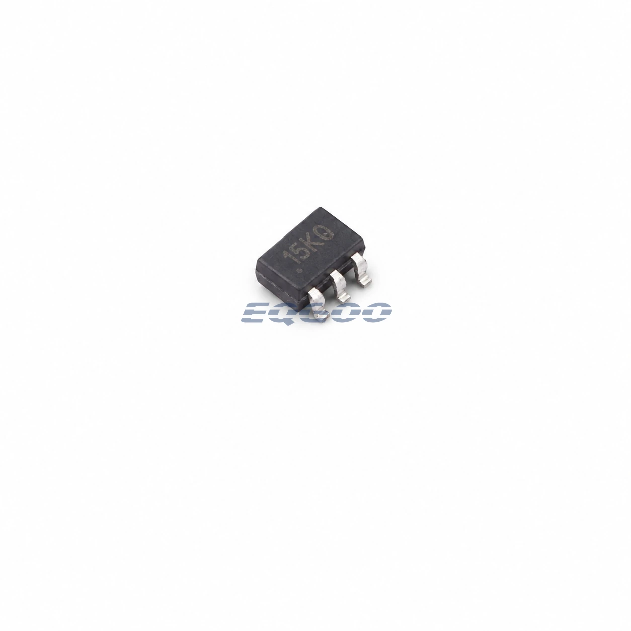
| RF impedance, port match, package, and pinout | Internally matched 50-ohm interface; at 1950 MHz input return loss 16.3 dB Typ and output return loss 15.4 dB Typ; six-lead SOT-363 with pin 3 RFIN and pin 6 RFOUT/bias (Return loss under default page 2 conditions; input/output DC-blocking capacitors required; bare base-device code has no packing form stated) | Determines PCB footprint, pinout, mechanical assembly and orderable-variant compatibility. |
| Exact Package | SOT-363 | Determines PCB footprint, pinout, mechanical assembly and orderable-variant compatibility. |
| Operating temperature and thermal path | TA -40 to +105 degC; TJ +125 degC Max; ?JC 126 degC/W Typ (Recommended operating envelope and junction-to-case thermal resistance) | Defines the thermal path and maximum recommended junction/ambient temperature envelope for safe use. |
| Absolute maximum and handling limits | Absolute max +4 V device voltage, 110 mA device current, +12 dBm RF input; HBM 2000 V Class 2; CDM C3; MSL 1 (Stress and handling limits, not normal operating targets; RF input limit applies with load impedance up to 10:1 VSWR) | Defines a selection-critical engineering characteristic that a compatible substitute must preserve under the stated conditions. |
RF Selection Notes
The device function and topology is Active-bias cascadable SiGe HBT Darlington MMIC amplifier; this defines the device function or architecture that a compatible replacement must preserve before secondary ratings are compared. Technical condition: Direct fixed 3 V operation with self-bias; no dropping resistor. 50 to 4000 MHz is the stated band coverage value. Defines the operating frequency or RF band that must cover the intended signal frequencies. Technical condition: Datasheet headline range; tabulated typical-performance points cover 500 to 3500 MHz and external coupling capacitors must be chosen for the operating frequency. Small-signal gain budget is 850 MHz 20.0 Min / 23.6 Typ; 1950 MHz 17.5 Min / 21.1 Typ; 2400 MHz 19.8 Typ dB. Sets the signal-level gain budget and must be compared at matching frequency, mode and bias conditions. Technical condition: VS 3 V, ID 48 mA typical, 25 degC, 50-ohm system unless otherwise noted; page 4 separately provides typical 500-to-3500-MHz application-circuit data. The compression headroom is 850 MHz +15.8 Typ; 1950 MHz +13.0 Min / +15.2 Typ; 2400 MHz +14.6 Typ dBm; this defines output compression headroom and must be compared at matching frequency and bias conditions. Technical condition: Default page 2 electrical test conditions; page 4 separately provides typical 500-to-3500-MHz application-circuit data. Third-order linearity is 850 MHz +29.0 Typ; 1950 MHz +25.0 Min / +27.8 Typ; 2400 MHz +26.6 Typ dBm. Defines third-order linearity headroom and must be compared with matching tone, frequency and bias conditions. Technical condition: VS 3 V, ID 48 mA typical, 25 degC, 50-ohm system; two tones spaced 1 MHz with 0 dBm output per tone.
2.5 Typ / 4.0 Max dB is the stated noise contribution value. Defines the device contribution to receiver noise and must be compared at matching frequency and bias conditions. Technical condition: 1950 MHz; VS 3 V, ID 48 mA typical, 25 degC, 50-ohm system unless otherwise noted.
Internally matched 50-ohm interface; at 1950 MHz input return loss 16.3 dB Typ and output return loss 15.4 dB Typ; six-lead SOT-363 with pin 3 RFIN and pin 6 RFOUT/bias is the stated rf impedance, port match, package, and pinout value. Determines PCB footprint, pinout, mechanical assembly and orderable-variant compatibility. Technical condition: Return loss under default page 2 conditions; input/output DC-blocking capacitors required; bare base-device code has no packing form stated.
Exact Package is SOT-363. Determines PCB footprint, pinout, mechanical assembly and orderable-variant compatibility.
At 3.0 V operating voltage Typ; 48 mA operating current Typ / 60 mA Max; self-bias with no dropping resistor, the supply and bias burden defines the required operating voltage and current together, setting board-rail compatibility, DC power demand and thermal burden. Technical condition: Normal operation; RFOUT is also the bias pin and requires DC blocking; 110 mA is an absolute maximum only. TA -40 to +105 degC; TJ +125 degC Max; ?JC 126 degC/W Typ is the stated operating temperature and thermal path value. Defines the thermal path and maximum recommended junction/ambient temperature envelope for safe use. Technical condition: Recommended operating envelope and junction-to-case thermal resistance.
Absolute max +4 V device voltage, 110 mA device current, +12 dBm RF input; HBM 2000 V Class 2; CDM C3; MSL 1 is the stated absolute maximum and handling limits value. Defines a selection-critical engineering characteristic that a compatible substitute must preserve under the stated conditions. Technical condition: Stress and handling limits, not normal operating targets; RF input limit applies with load impedance up to 10:1 VSWR.