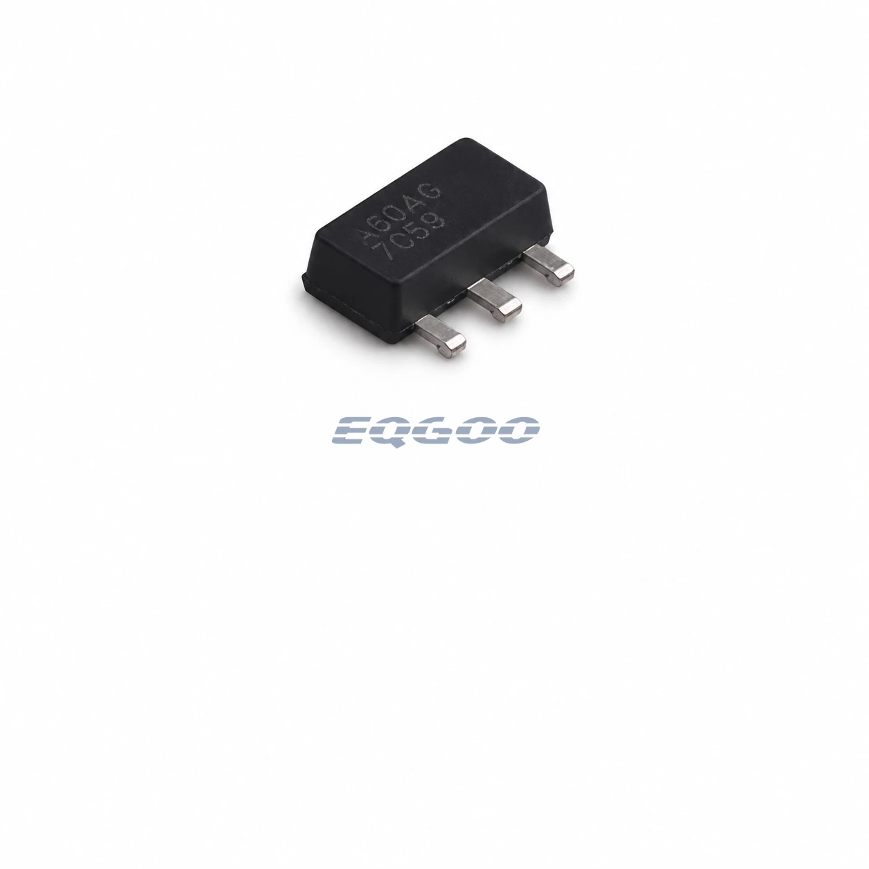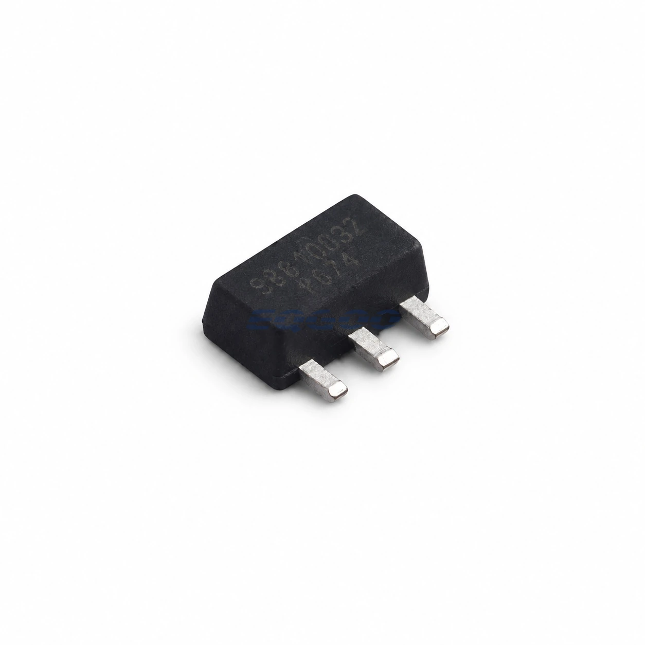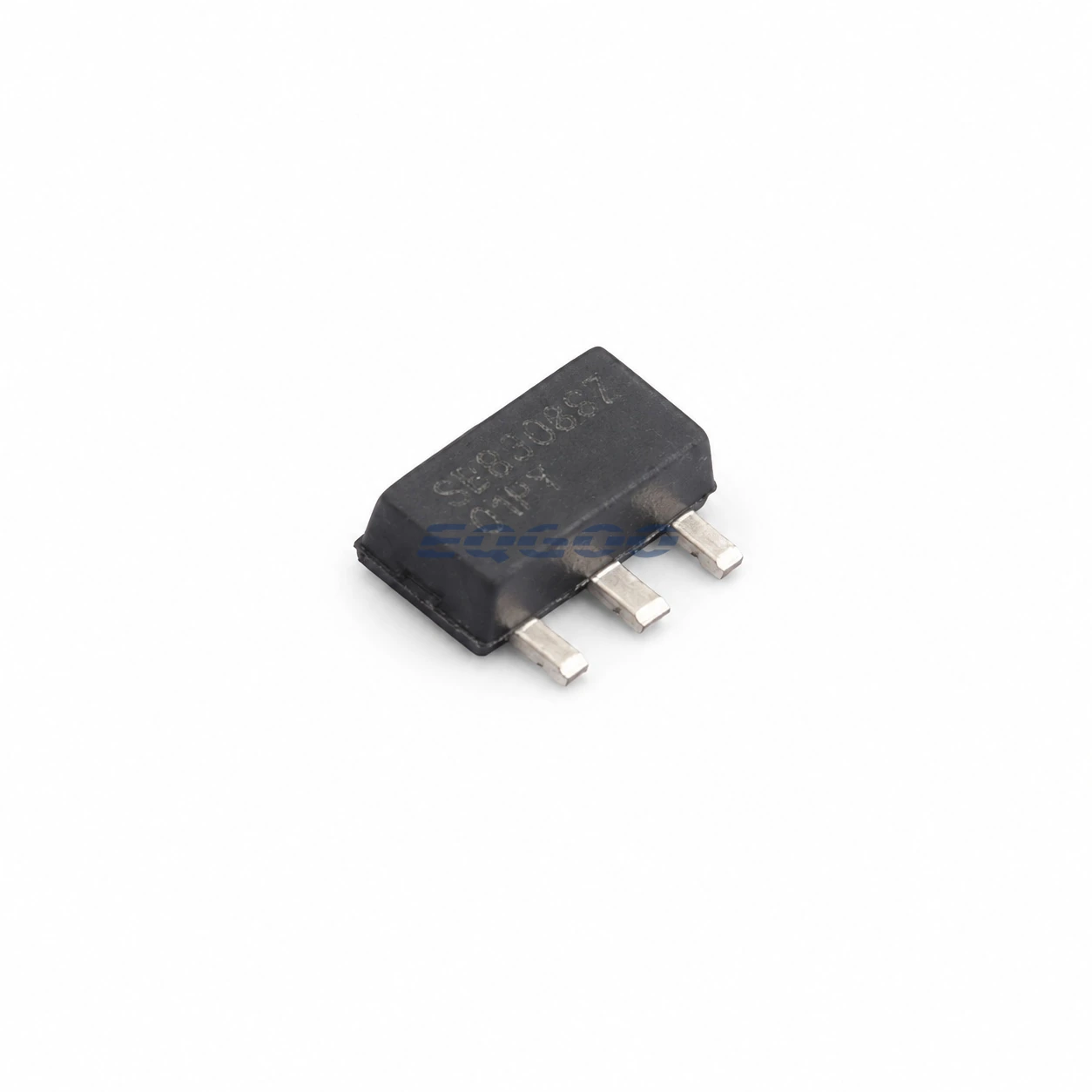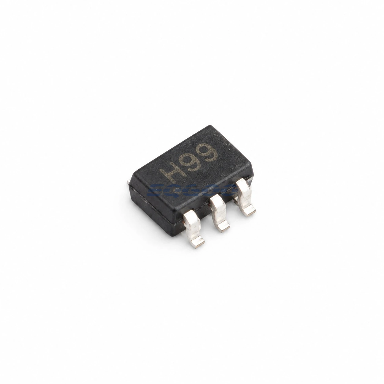
Device Overview
Designed as a General-purpose InGaP/GaAs HBT Darlington-pair RF buffer/gain block, Qorvo AG203-63G uses the SOT-363 package. The main engineering checks for this variant are Device function and topology (General-purpose InGaP/GaAs HBT Darlington-pair RF buffer/gain block), Operational frequency range (DC to 6000 MHz), Small-signal gain (19.7 typical (rounded to +20 in Key Features) dB).
Selection-Critical Data
| Parameter | Confirmed Data | Why It Matters |
|---|---|---|
| Device function and topology | General-purpose InGaP/GaAs HBT Darlington-pair RF buffer/gain block (AG203-63 family device represented by the exact AG203-63G ordering part) | Defines the device function or architecture that a compatible replacement must preserve before secondary ratings are compared. |
| Operational frequency range | DC to 6000 MHz (Electrical-specification range; actual band implementation depends on external component values) | Defines the operating frequency or RF band that must cover the intended signal frequencies. |
| Small-signal gain | 19.7 typical (rounded to +20 in Key Features) dB (900 MHz; VSUPPLY 5.0 V, RBIAS 47.5 ohm, 25 degrees C, 50-ohm system unless otherwise noted) | Sets the signal-level gain budget and must be compared at matching frequency, mode and bias conditions. |
| Output 1 dB compression point | +8 typical dBm (900 MHz; VSUPPLY 5.0 V, RBIAS 47.5 ohm, 25 degrees C, 50-ohm system unless otherwise noted) | Defines output compression headroom and must be compared at matching frequency and bias conditions. |
| Output third-order intercept | +20.1 typical (rounded to +20 in Key Features) dBm (900 MHz; two output tones at -10 dBm per tone separated by 10 MHz; largest IMD3 product with 2:1 calculation; default page 2 bias conditions) | Defines third-order linearity headroom and must be compared with matching tone, frequency and bias conditions. |
| Noise figure | 3.0 typical dB (900 MHz; VSUPPLY 5.0 V, RBIAS 47.5 ohm, 25 degrees C, 50-ohm system unless otherwise noted) | Defines the device contribution to receiver noise and must be compared at matching frequency and bias conditions. |
| Supply and nominal bias | VSUPPLY 4.75 / 5.00 / 5.25 V min/typ/max; VDEVICE 4.05 V typical; ICC 20 mA typical | Defines the required supply voltage and bias current together, which sets both rail compatibility and DC/thermal burden. |
| RF interface and matching | Internally matched to 50 ohms; input return loss 20 dB typical and output return loss 16 dB typical at 900 MHz (Return-loss values at 900 MHz under default page 2 electrical test conditions) | Defines the 50-ohm RF matching behavior of the amplifier input/output; this is an RF interface, not a digital host interface. |
| Exact package, pinout and packing | SOT-363, 6 pins; pin 3 RF input, pin 6 RF output/bias, four ground pins; standard 3000-piece 7-inch reel (Exact AG203-63G ordering entry for packing) | Determines PCB footprint, pinout, mechanical assembly and orderable-variant compatibility. |
| External bias and band network | DC-blocking capacitors, bias resistor and inductive RF choke required; values depend on desired frequency band (Manufacturer integration guidance; evaluation-board BOM values are example configurations rather than universal values) | Defines the operating frequency or RF band that must cover the intended signal frequencies. |
| Thermal path and stress limits | Theta-JC 472 degrees C/W; absolute maximum VDEVICE 4.5 V, RF input +10 dBm CW, TJ 177 degrees C (RF input limit in a 50-ohm system at 25 degrees C; absolute maxima are stress limits, not operating targets) | Defines the thermal path and absolute stress limits that constrain safe operating temperature, voltage and RF input power. |
| ESD, compliance and reflow | 1000 V HBM Class 1C; lead-free / green / RoHS-compliant; 260 degrees C maximum lead-free reflow (Claims are from the dated 2019 datasheet; tin/lead reflow maximum is 245 degrees C) | Defines a selection-critical engineering characteristic that a compatible substitute must preserve under the stated conditions. |
| Lifecycle / Procurement | Production | Supports current sourcing and new-design consideration. |
RF Selection Notes
At General-purpose InGaP/GaAs HBT Darlington-pair RF buffer/gain block, the device function and topology defines the device function or architecture that a compatible replacement must preserve before secondary ratings are compared. Technical condition: AG203-63 family device represented by the exact AG203-63G ordering part. At DC to 6000 MHz, the operational frequency range defines the operating frequency or RF band that must cover the intended signal frequencies. Technical condition: Electrical-specification range; actual band implementation depends on external component values. External bias and band network is DC-blocking capacitors, bias resistor and inductive RF choke required; values depend on desired frequency band. Defines the operating frequency or RF band that must cover the intended signal frequencies. Technical condition: Manufacturer integration guidance; evaluation-board BOM values are example configurations rather than universal values.
19.7 typical (rounded to +20 in Key Features) dB is the stated small-signal gain value. Sets the signal-level gain budget and must be compared at matching frequency, mode and bias conditions. Technical condition: 900 MHz; VSUPPLY 5.0 V, RBIAS 47.5 ohm, 25 degrees C, 50-ohm system unless otherwise noted. For noise figure, 3.0 typical dB is the approved value. Defines the device contribution to receiver noise and must be compared at matching frequency and bias conditions. Technical condition: 900 MHz; VSUPPLY 5.0 V, RBIAS 47.5 ohm, 25 degrees C, 50-ohm system unless otherwise noted.
Output 1 dB compression point is +8 typical dBm. Defines output compression headroom and must be compared at matching frequency and bias conditions. Technical condition: 900 MHz; VSUPPLY 5.0 V, RBIAS 47.5 ohm, 25 degrees C, 50-ohm system unless otherwise noted. For output third-order intercept, +20.1 typical (rounded to +20 in Key Features) dBm is the approved value. Defines third-order linearity headroom and must be compared with matching tone, frequency and bias conditions. Technical condition: 900 MHz; two output tones at -10 dBm per tone separated by 10 MHz; largest IMD3 product with 2:1 calculation; default page 2 bias conditions.
At Internally matched to 50 ohms; input return loss 20 dB typical and output return loss 16 dB typical at 900 MHz, the rf interface and matching defines the documented control or communication path that must remain compatible with the host and surrounding peripherals. Technical condition: Return-loss values at 900 MHz under default page 2 electrical test conditions.
SOT-363, 6 pins; pin 3 RF input, pin 6 RF output/bias, four ground pins; standard 3000-piece 7-inch reel is the stated exact package, pinout and packing value. Determines PCB footprint, pinout, mechanical assembly and orderable-variant compatibility. Technical condition: Exact AG203-63G ordering entry for packing.
Supply and nominal bias is VSUPPLY 4.75 / 5.00 / 5.25 V min/typ/max; VDEVICE 4.05 V typical; ICC 20 mA typical. Defines the required supply voltage and bias current together, which sets both rail compatibility and DC/thermal burden. Thermal path and stress limits is Theta-JC 472 degrees C/W; absolute maximum VDEVICE 4.5 V, RF input +10 dBm CW, TJ 177 degrees C. Defines the thermal path and absolute stress limits that constrain safe operating temperature, voltage and RF input power. Technical condition: RF input limit in a 50-ohm system at 25 degrees C; absolute maxima are stress limits, not operating targets.
1000 V HBM Class 1C; lead-free / green / RoHS-compliant; 260 degrees C maximum lead-free reflow is the stated esd, compliance and reflow value. Defines a selection-critical engineering characteristic that a compatible substitute must preserve under the stated conditions. Technical condition: Claims are from the dated 2019 datasheet; tin/lead reflow maximum is 245 degrees C.
Engineering Resource
For higher output compression and linearity in a DC–6 GHz Qorvo SOT-363 gain block, compare AG303-63G with this AG203-63G. Qorvo specifies approximately +14 dBm versus +8 dBm output P1dB and +26 dBm versus +21 dBm OIP3 at 900 MHz for AG303-63G and AG203-63G, respectively. The devices also have different bias-current requirements; evaluate DC bias, matching and thermal design rather than assuming direct interchangeability.