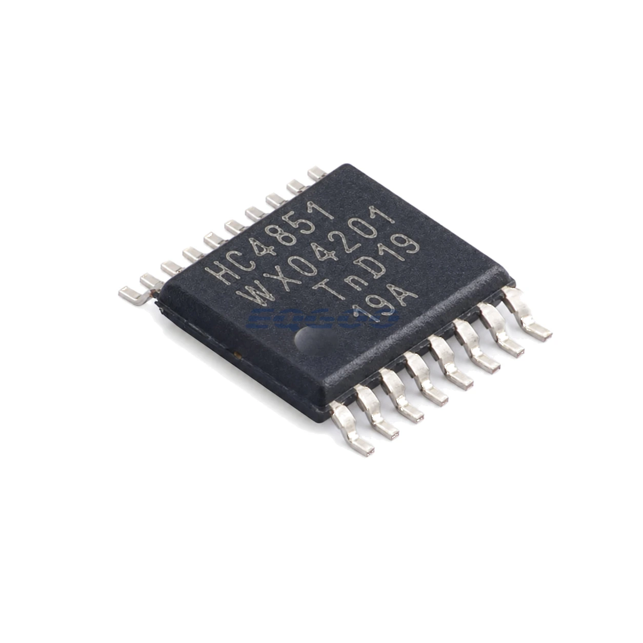
Key Selection Information
| Selection Parameter | Confirmed Information |
|---|---|
| Manufacturer | Nexperia |
| Exact MPN | 74HC4851PW-Q100,11 |
| Product Category | Signal Switches, Multiplexers, Decoders |
| Package | TSSOP-16 |
| Packing | 2,500 pcs/reel |
| Supply Polarity | Single supply |
| Operating Voltage | 2V to 6V |
| Inputs / Outputs | 3/8 |
| Operating Temperature | -40℃ to +125℃ |
Product Overview
Automotive-qualified 8-channel analog multiplexer/demultiplexer with injection-current effect control; SP8T-Z configuration, three select inputs, active-LOW enable, eight Y0–Y7 channels, and common Z.
RON falls substantially as supply increases, so channel resistance and signal attenuation must be evaluated at the actual rail. Injection-current control is useful where disabled channels can exceed the supply, but it does not remove the specified voltage/current limits.
Technical Specifications
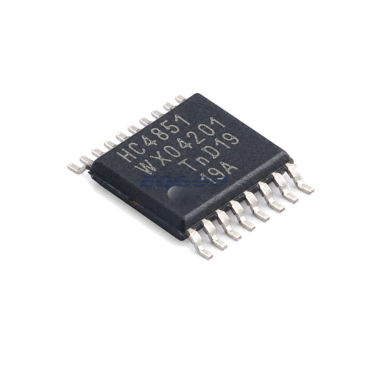
| Parameter | Verified Information |
|---|---|
| Manufacturer | Nexperia |
| Exact MPN | 74HC4851PW-Q100,11 |
| Functional Category | Signal Switches, Multiplexers, Decoders |
| Package | TSSOP-16 |
| Packing | 2,500 pcs/reel |
| Source Catalog ID | C458225 |
| Supply Polarity | Single supply |
| Operating Voltage | 2V to 6V |
| Inputs / Outputs | 3/8 |
| Operating Temperature | -40℃ to +125℃ |
Selection Notes
HC versus HCT thresholds; automotive qualification; RON versus supply; injection-current behavior; TSSOP16 versus other packages; analog bandwidth/load requirements.
Confirm the exact switching/decoding function, channel topology, logic voltage and on-state or output-drive constraints.
Manufacturer Decision-Relevant Notes
Supply: 2.0–6.0 V. ; Operating temperature: -40 to +125 °C. ; Typical RON: 400 Ω at 2.0 V, 215 Ω at 3.0 V, 120 Ω at 3.3 V, 76 Ω at 4.5 V, 59 Ω at 6.0 V. ; Product-table RON: 220 Ω. ; Injection-current cross-coupling: <1 mV/mA. ; Input/switch voltage: 0 to VCC. ; Input transition-rate limit, HC: typ 6 ns/V, max 1000 ns/V at 2.0 V, 800 ns/V at 3.0/3.3 V, 500 ns/V at 4.5 V, 400 ns/V at 6.0 V. ; ESD: HBM >2 kV; CDM >1 kV.
Design Considerations
-
- Calculate worst-case gain error and RC settling using the applicable RON at the actual VCC, temperature, and signal load. 2. Verify each analog signal remains within the specified 0–VCC switch-voltage range unless the datasheet’s injection-current conditions explicitly apply. 3. Check select and enable rise/fall times against the stated transition-rate limits. 4. Verify AEC-Q100 Grade 1 documentation and automotive temperature requirement for the program. 5. Confirm the TSSOP16 SOT403-1 footprint and thermal design.
Application Fit
Digital multiplexing/demultiplexing, signal gating, and automotive signal routing.
Manufacturer Resources
Quality & Verification Support
Third-party inspection or testing can be arranged according to customer requirements. Testing fees are borne by the buyer. Additional verification requirements can be discussed before shipment. Physical product, label, packaging, and Date Code photos may be provided where appropriate.
Request a Quote
For 74HC4851PW-Q100,11 quotation, provide the exact MPN, required quantity, destination, target Date Code if applicable, and any inspection or testing requirements.