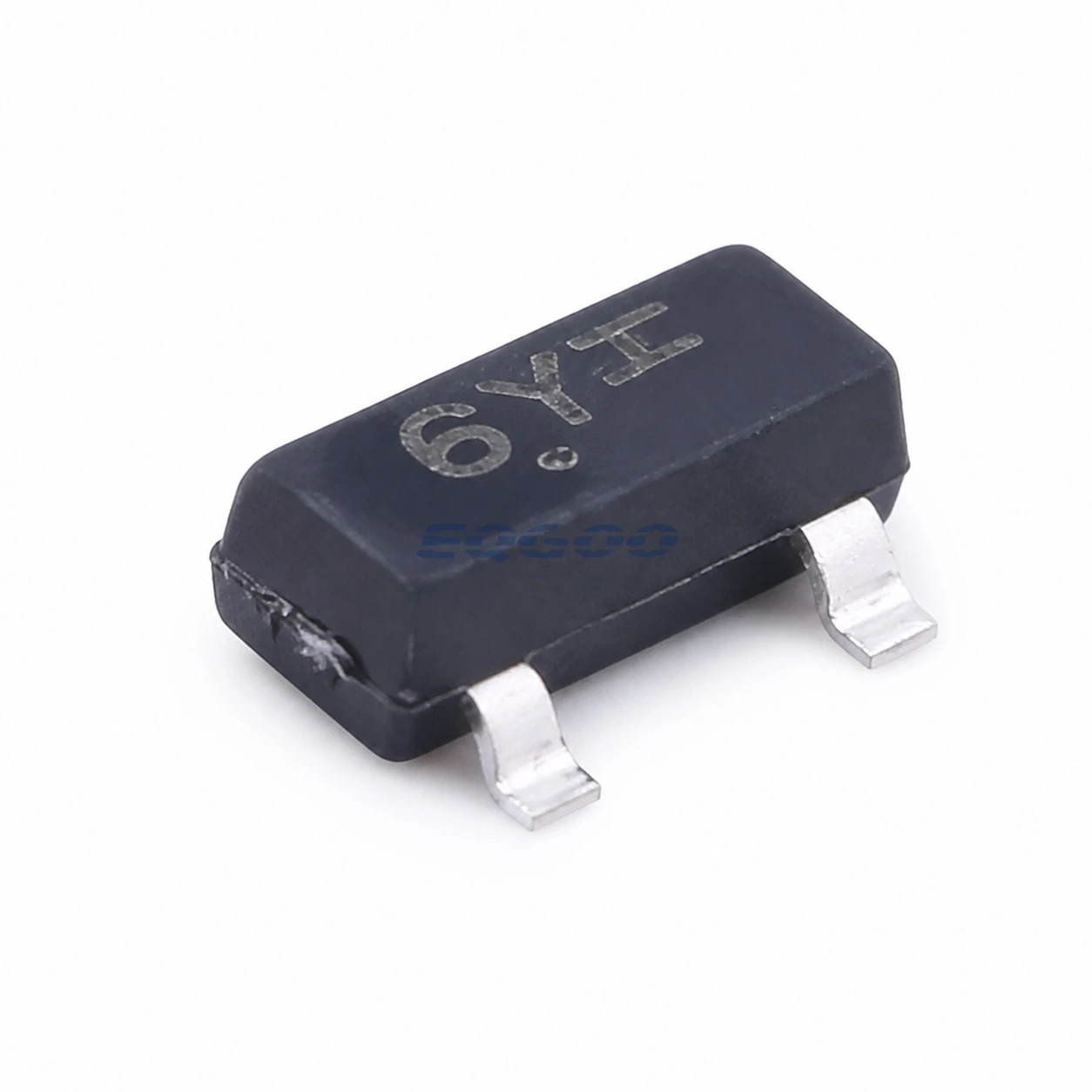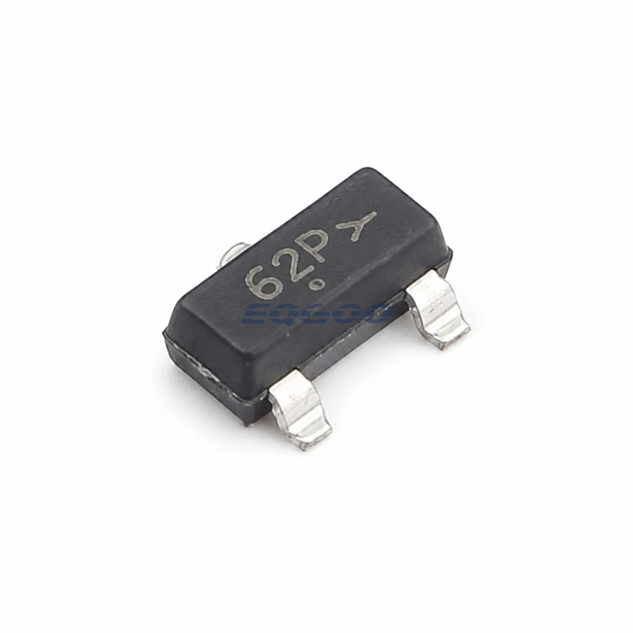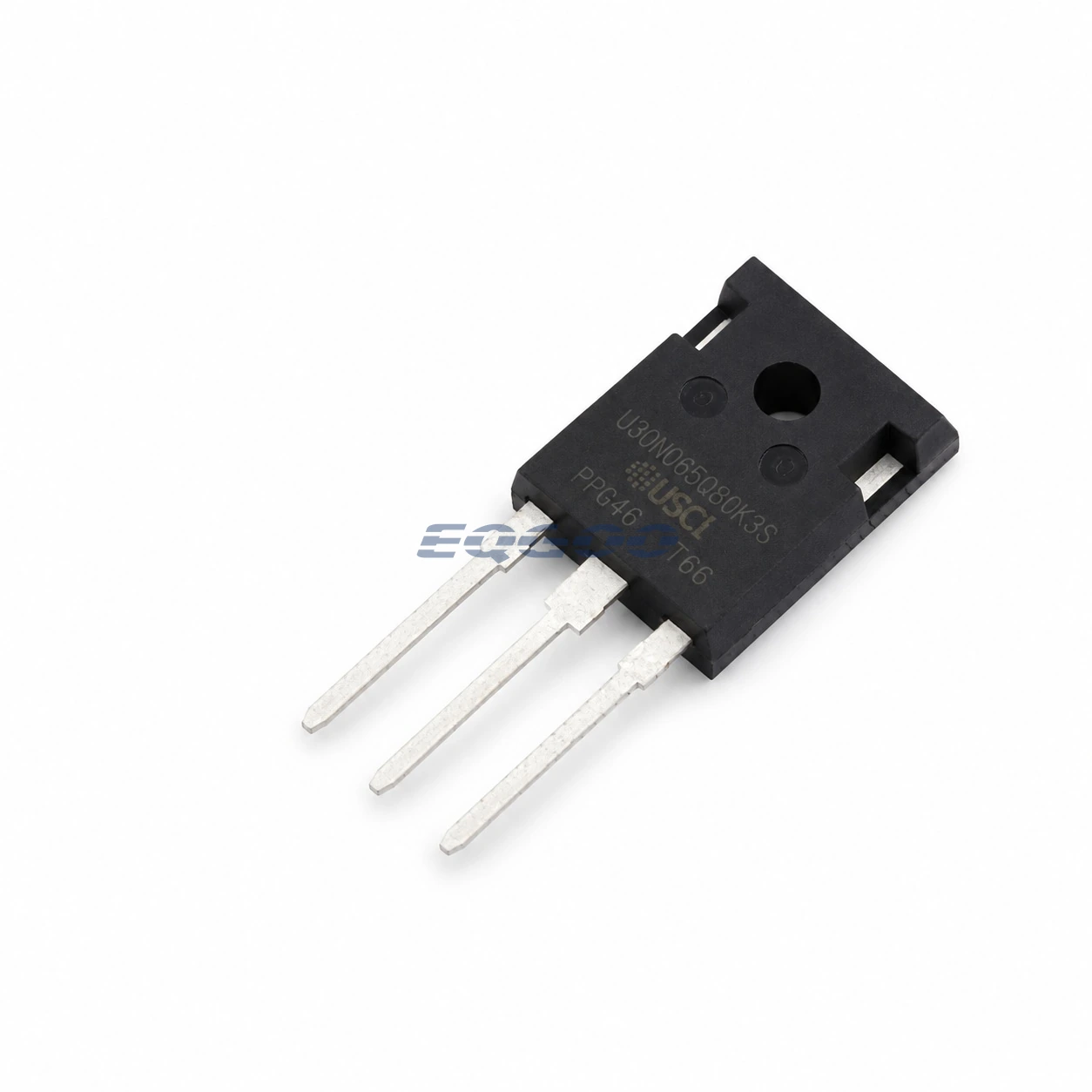
Device Overview
Designed as a Normally-off SiC FET; cascode of normally-on SiC JFET and low-voltage Si MOSFET, Qorvo UF3SC065030D8S uses the DFN8X8-4L package. Selection of this exact part is driven primarily by Device type and switching architecture, Drain-source blocking voltage (650 V), On-state resistance across temperature (34 typ / 42 max at 25 degC; 48 typ / 55 max at 150 degC mOhm).
Selection-Critical Data
| Parameter | Confirmed Data | Why It Matters |
|---|---|---|
| Device type and switching architecture | Normally-off Gen 3 FAST SiC FET using a cascode of a normally-on SiC JFET and low-voltage Si MOSFET (External behavior is enhancement-mode; architecture is internal to the co-package) | Defines the device function or architecture that a compatible replacement must preserve before secondary ratings are compared. |
| Drain-source blocking voltage | 650 V (Absolute maximum VDS; circuit working voltage and transients require design margin below this limit) | Defines the electrical voltage envelope that must cover the intended operating or stress level. |
| On-state resistance across temperature | 34 typ / 42 max at 25 degC; 48 typ / 55 max at 150 degC mOhm (VGS = 12 V and ID = 20 A; values are specified at TJ = 25 degC and 150 degC respectively) | Affects conduction loss and heat generation under the stated current, gate-drive and temperature conditions. |
| Drain-current capability | 18 continuous; 160 pulsed A (18 A at TC < 134 degC and limited by bondwires; 160 A at TC = 25 degC with pulse width limited by TJ,max) | Defines the current-handling or drive capability that must meet the load while respecting current-path and thermal limits. |
| Gate-voltage interface | VGS absolute maximum -25 to +25 V; VGS(th) 4 min / 5 typ / 6 max V; RDS(on) specified at VGS = 12 V (VGS limit is DC; threshold is measured at VDS = 5 V and ID = 10 mA and must not be used as a full-on drive target) | Defines gate-drive compatibility and protection limits; threshold voltage is not a full-on gate-drive target. |
| Gate charge and small-signal capacitances | Qg 43 nC; Ciss 1500 pF; Coss 320 pF; Crss 2.3 pF mixed (Qg: VDS = 400 V, ID = 20 A, VGS = -5 V to +12 V; capacitances: VDS = 100 V, VGS = 0 V, f = 100 kHz; all typical) | Affects gate-drive energy, switching-transition demand and switching-loss tradeoffs. |
| Junction-to-case thermal path and temperature ceiling | RthetaJC 0.54 typ / 0.7 max degC/W; TJ,max 150 degC; Ptot 179 W at TC = 25 degC mixed (Junction-to-case thermal resistance; power dissipation is a case-temperature-conditioned maximum and must be derated) | Defines junction-to-case thermal resistance, power-dissipation capability and the temperature ceiling that must be respected in thermal design. |
| Exact package and Kelvin-source pinout | DFN8X8-4L; D=tab, S=pins 3/4, G=pin 1, KS=pin 2 (Surface-mount 8 mm x 8 mm package with separate Kelvin-source gate return) | Determines PCB footprint, pinout, mechanical assembly and orderable-variant compatibility. |
| Lifecycle and sourcing status | Obsolete/discontinued; LTB 2021-10-29; LTS 2021-12-29 (Manufacturer PCN cites DFN8 subcontractor line shutdown and gives no alternate part) | Affects procurement continuity and the risk of selecting the part for a new design. |
| Single-pulse avalanche energy | 120 mJ (L = 15 mH, IAS = 4 A, starting TJ = 25 degC) | Defines a selection-critical engineering characteristic that a compatible substitute must preserve under the stated conditions. |
Power-Device Selection Notes
At 34 typ / 42 max at 25 degC; 48 typ / 55 max at 150 degC mOhm, the on-state resistance across temperature affects conduction loss and heat generation under the stated current, gate-drive and temperature conditions. Technical condition: VGS = 12 V and ID = 20 A; values are specified at TJ = 25 degC and 150 degC respectively.
The junction-to-case thermal path and temperature ceiling is RthetaJC 0.54 typ / 0.7 max degC/W; TJ,max 150 degC; Ptot 179 W at TC = 25 degC mixed; this defines functional logic or signal-routing behavior; a substitute must preserve the required truth table, direction and control-state behavior. Technical condition: Junction-to-case thermal resistance; power dissipation is a case-temperature-conditioned maximum and must be derated.
At DFN8X8-4L; D=tab, S=pins 3/4, G=pin 1, KS=pin 2, the exact package and kelvin-source pinout determines PCB footprint, pinout, mechanical assembly and orderable-variant compatibility. Technical condition: Surface-mount 8 mm x 8 mm package with separate Kelvin-source gate return.
At Normally-off Gen 3 FAST SiC FET using a cascode of a normally-on SiC JFET and low-voltage Si MOSFET, the device type and switching architecture defines the device function or architecture that a compatible replacement must preserve before secondary ratings are compared. Technical condition: External behavior is enhancement-mode; architecture is internal to the co-package. Drain-source blocking voltage is 650 V. Defines the electrical voltage envelope that must cover the intended operating or stress level. Technical condition: Absolute maximum VDS; circuit working voltage and transients require design margin below this limit.
For drain-current capability, 18 continuous; 160 pulsed A is the approved value. Defines the current-handling or drive capability that must meet the load while respecting current-path and thermal limits. Technical condition: 18 A at TC < 134 degC and limited by bondwires; 160 A at TC = 25 degC with pulse width limited by TJ,max. Gate-voltage interface is VGS absolute maximum -25 to +25 V; VGS(th) 4 min / 5 typ / 6 max V; RDS(on) specified at VGS = 12 V. Defines gate-drive compatibility and protection limits; threshold voltage is not a full-on gate-drive target. Technical condition: VGS limit is DC; threshold is measured at VDS = 5 V and ID = 10 mA and must not be used as a full-on drive target.
The gate charge and small-signal capacitances is Qg 43 nC; Ciss 1500 pF; Coss 320 pF; Crss 2.3 pF mixed; this affects gate-drive energy, switching-transition demand and switching-loss tradeoffs. Technical condition: Qg: VDS = 400 V, ID = 20 A, VGS = -5 V to +12 V; capacitances: VDS = 100 V, VGS = 0 V, f = 100 kHz; all typical. For single-pulse avalanche energy, 120 mJ is the approved value. Defines a selection-critical engineering characteristic that a compatible substitute must preserve under the stated conditions. Technical condition: L = 15 mH, IAS = 4 A, starting TJ = 25 degC.
The lifecycle and sourcing status is Obsolete/discontinued; LTB 2021-10-29; LTS 2021-12-29; this affects procurement continuity and the risk of selecting the part for a new design. Technical condition: Manufacturer PCN cites DFN8 subcontractor line shutdown and gives no alternate part.
For the same Qorvo/UnitedSiC 650 V cascode SiC FET in DFN8x8-4L with a higher on-state resistance class, compare UF3SC065040D8S with this UF3SC065030D8S. Manufacturer data for this DFN8x8-4L pair lists about 34 mΩ typical RDS(on) at 25 °C (VGS=12 V) for UF3SC065030D8S versus a 42 mΩ RDS(on) device class for UF3SC065040D8S, so conduction-loss and thermal-budget requirements differ even though both are 650 V cascode FETs in the same package family. Compare RDS(on) at your junction temperature and switching conditions; shared package naming alone does not by itself establish electrical equivalence.