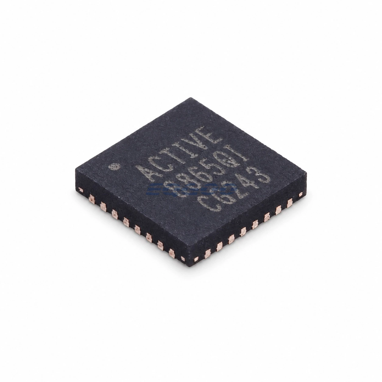
Device Overview
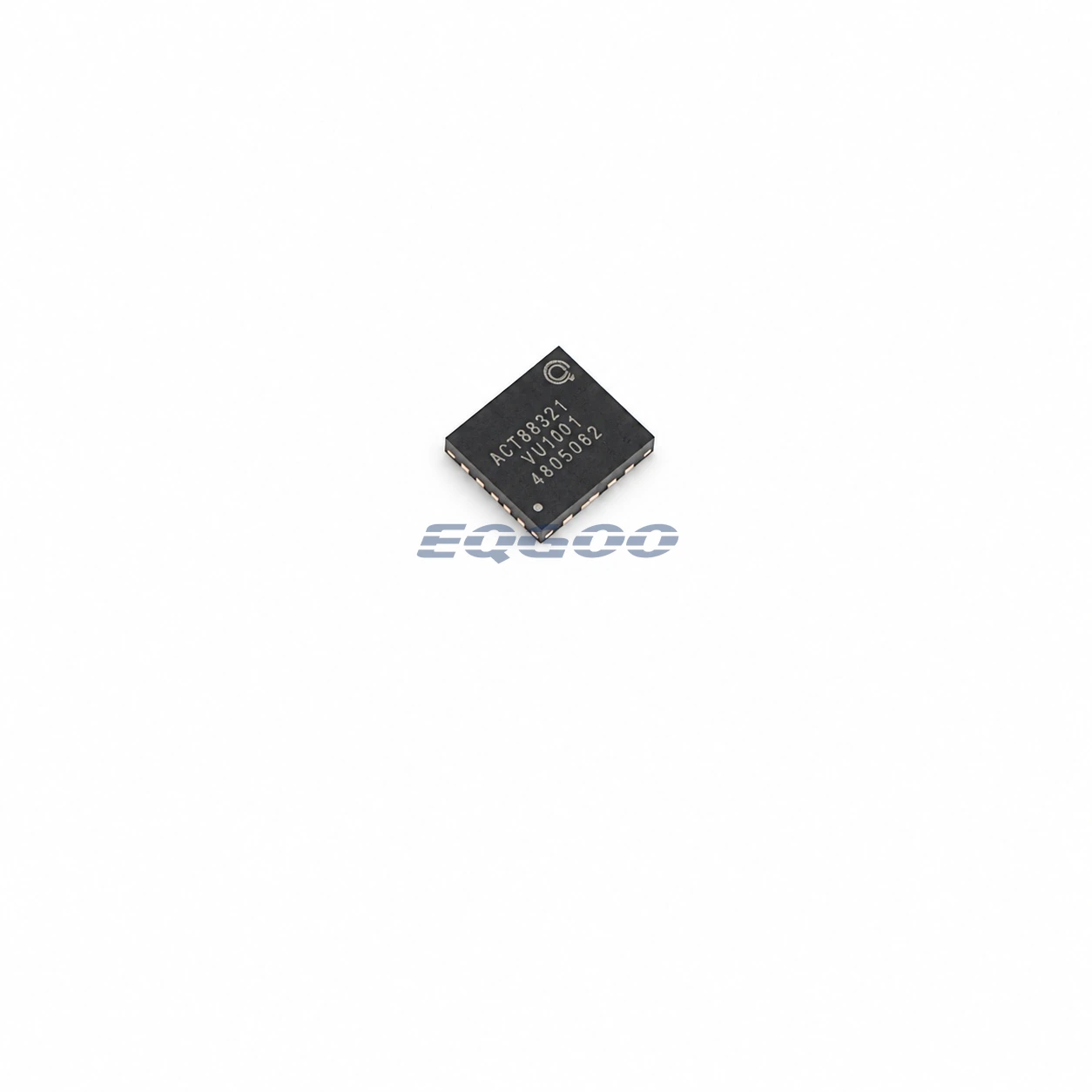
ACT8865QI305-T is a Qorvo PMIC with buck regulators, LDOs and sequencing in a 32-pin TQFN, 4.0 x 4.0 mm package. The main engineering checks for this variant are Device Function (PMIC with buck regulators, LDOs and sequencing), Input Voltage (2.7 to 5.5 V), Output Current (1300 mA).
Selection-Critical Data
| Parameter | Confirmed Data | Why It Matters |
|---|---|---|
| Device Function | PMIC with buck regulators, LDOs and sequencing | Defines the device function or architecture that a compatible replacement must preserve before secondary ratings are compared. |
| Input Voltage | 2.7 to 5.5 V | Defines compatibility with the available system input rail and its operating range. |
| Output Current | 1300 mA | Defines the current-handling or drive capability that must meet the load while respecting current-path and thermal limits. |
| Exact Package | 32-pin TQFN, 4.0 x 4.0 mm | Determines PCB footprint, pinout, mechanical assembly and orderable-variant compatibility. |
| Regulated Outputs | 7 total regulated outputs | Qorvo’s current page agrees on seven outputs but contains an internal buck/LDO count conflict, so the exact split is not asserted here. |
| Interfaces | I2C | Defines the documented control or communication path that must remain compatible with the host and surrounding peripherals. |
| Operating Temperature | -40 to 125 degC | Defines the qualified measurement or environmental range that the design must remain within. |
| Switching Frequency | 2 MHz fixed-frequency DC/DC architecture | Defines the converter switching rate and affects passive-component sizing, ripple and EMI. |
| Lifecycle / Procurement | Production | Supports current sourcing; exact rail configuration should be checked for the QI305 option. |
Power-Management Selection Notes
PMIC with buck regulators, LDOs and sequencing is the stated device function value. Defines the device function or architecture that a compatible replacement must preserve before secondary ratings are compared. At 2.7 to 5.5 V, the input voltage defines compatibility with the available system input rail and its operating range. At 1300 mA, the output current defines the current-handling or drive capability that must meet the load while respecting current-path and thermal limits.
Interfaces is I2C. Defines the documented control or communication path that must remain compatible with the host and surrounding peripherals.
For operating temperature, -40 to 125 degC is the approved value. Defines the qualified measurement or environmental range that the design must remain within.
Exact Package is 32-pin TQFN, 4.0 x 4.0 mm. Determines PCB footprint, pinout, mechanical assembly and orderable-variant compatibility.
For regulator resources, 4 buck converters, 3 LDO regulators is the approved value. Defines a selection-critical engineering characteristic that a compatible substitute must preserve under the stated conditions.