Device Character
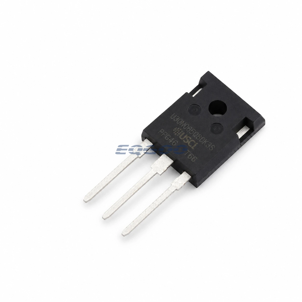
UJ3N065080K3S is a 650 V normally-on silicon-carbide JFET in a TO-247-3L package. Its default conduction behavior is a key selection point: the device is normally on at VGS = 0 V. Under VGS = 0 V, ID = 10 A and TJ = 25 °C, the datasheet specifies 80 mΩ typical RDS(on).
Key Power-Device Data
| Parameter | Confirmed Information | Conditions |
|---|---|---|
| Device type | Normally-on SiC JFET | Conducting characteristic at VGS = 0 V |
| Drain-source voltage | 650 V | |
| RDS(on), typical | 80 mΩ | VGS = 0 V, ID = 10 A, TJ = 25 °C |
| Total gate charge, typical | 75 nC | VDS = 400 V, ID = 24 A, VGS = -18 V to 0 V |
| Maximum junction temperature | 175 °C | |
| Thermal resistance, junction-to-case | 0.61 °C/W typ, 0.79 °C/W max | |
| Package | TO-247-3L |
Gate-Drive and Replacement Considerations
The normally-on characteristic should be checked before treating another 650 V device as a substitute. The manufacturer characterizes switching with negative gate bias, including -18 V to 0 V conditions, so an existing gate-drive arrangement should be reviewed for compatibility with this device behavior.
The 80 mΩ typical on-resistance, 75 nC typical gate charge and junction-to-case thermal resistance address different parts of the design trade-off. They should be considered together rather than comparing only voltage class and package.
Application Context
The manufacturer datasheet lists over-current protection circuits, DC-AC inverters, switch-mode power supplies, power-factor-correction modules, motor drives and induction heating among the application areas for this device.
Engineering Resource
For lower typical on-resistance in the 650 V normally-on SiC JFET family, compare UJ3N065025K3S (25 mΩ) with this UJ3N065080K3S (80 mΩ); both are TO-247-3L orderables. Qorvo’s selection guide also lists different 25°C drain-current classes. Confirm the applicable RDS(on) test conditions, gate-drive handling and thermal design before selecting the other device.