Key Selection Information
| Selection Parameter | Confirmed Information |
|---|---|
| Device type | N-channel JFET analog switch |
| Intended use | Low-level analog switching, sample/hold and chopper circuits |
| Gate-source breakdown | −35 V minimum magnitude |
| J113 cutoff range | −0.5 V to −3.0 V |
| J113 IDSS | 2 mA minimum |
| J113 RDS(on) | 100 Ω maximum at the stated low-voltage test |
| Source/drain | Interchangeable |
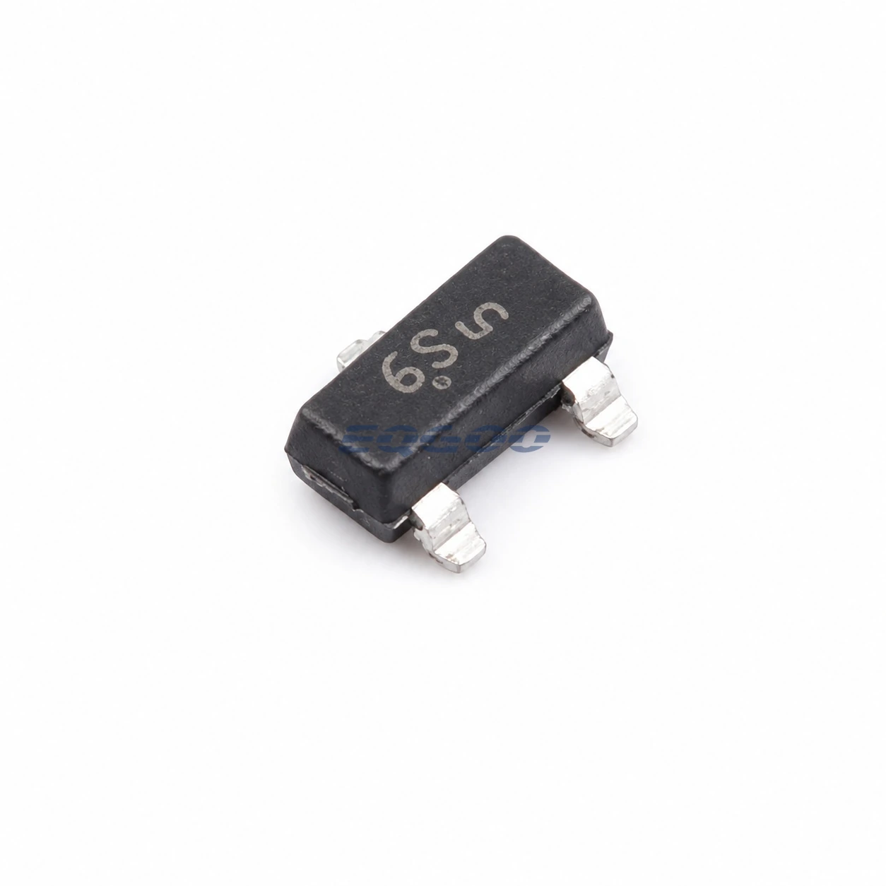
| Package | SOT-23 |
| Junction range | −55°C to +150°C |
Product Overview
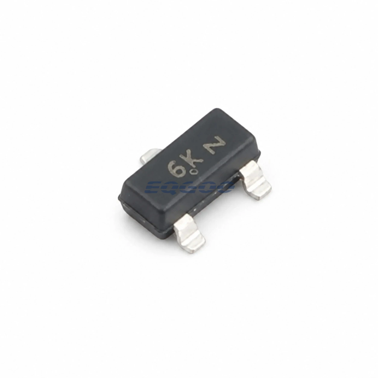
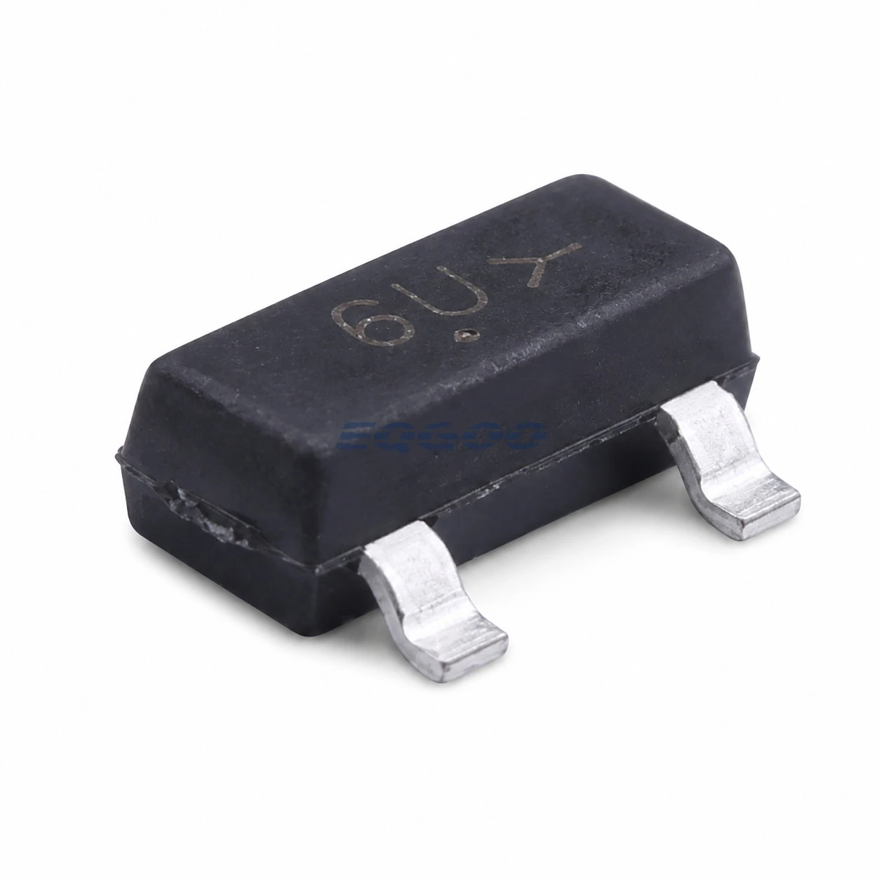
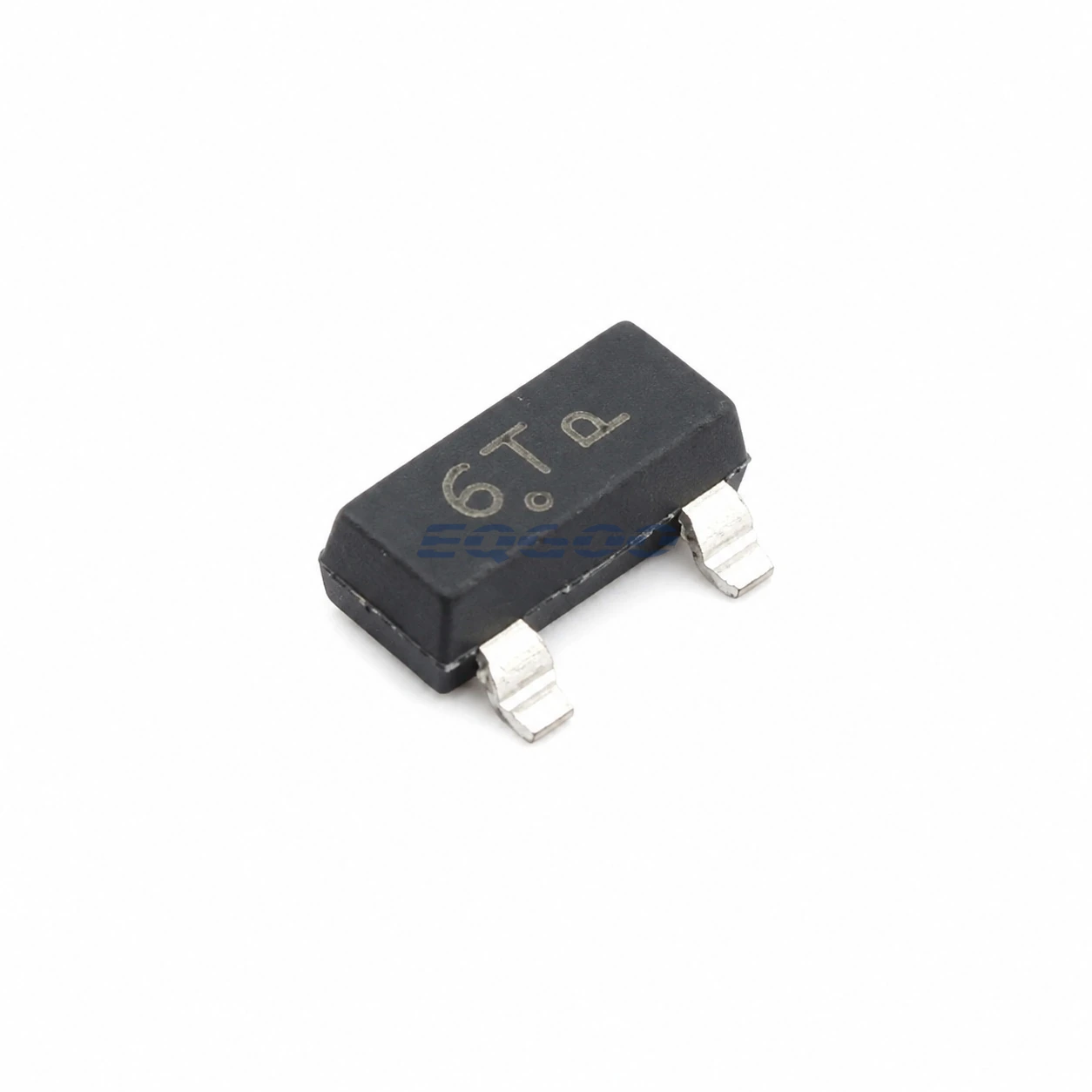
MMBFJ113 is the SOT-23 surface-mount version of onsemi’s J113 N-channel JFET switch. It is intended for low-level analog switching, sample-and-hold circuits and chopper-stabilized amplifier functions where the JFET’s normally-on behavior and analog bidirectionality are useful.
Compared with the related J111 and J112 grades, the J113 has the lowest-magnitude cutoff-voltage range, specified at approximately −0.5 V to −3.0 V under the datasheet test condition.
Technical Specifications
| Parameter | Confirmed Information |
|---|---|
| Channel | N-channel |
| V(BR)GSS | −35 V minimum magnitude |
| VGS(off), J113 | −0.5 V to −3.0 V |
| IDSS, J113 | 2 mA minimum |
| RDS(on), J113 | 100 Ω maximum at VGS = 0 test |
| Gate reverse current | 1 nA maximum at stated test condition |
| Source/drain interchange | Yes |
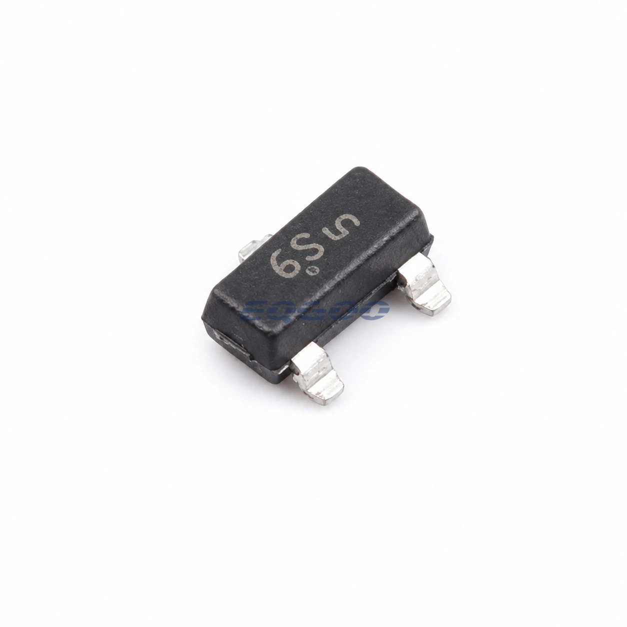
| Package | SOT-23 |
| Maximum device dissipation | 350 mW under stated board condition |
JFET Switching Considerations
MMBFJ113 is a normally-on depletion device: applying reverse gate bias reduces channel conduction. The gate-control range and source/drain signal swing therefore need to be checked together so the channel reaches the intended on and off states without forward-biasing the gate junction.
Manufacturer Resource
Quality & Verification Support
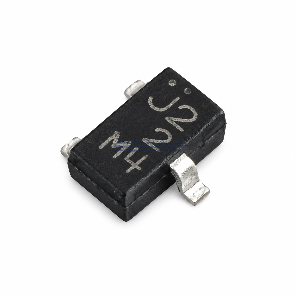
Exact MMBFJ113 marking, SOT-23 package, lot/date information and packing can be reviewed before shipment.
Request a Quote
Request MMBFJ113 exactly and include quantity, date-code and traceability requirements.