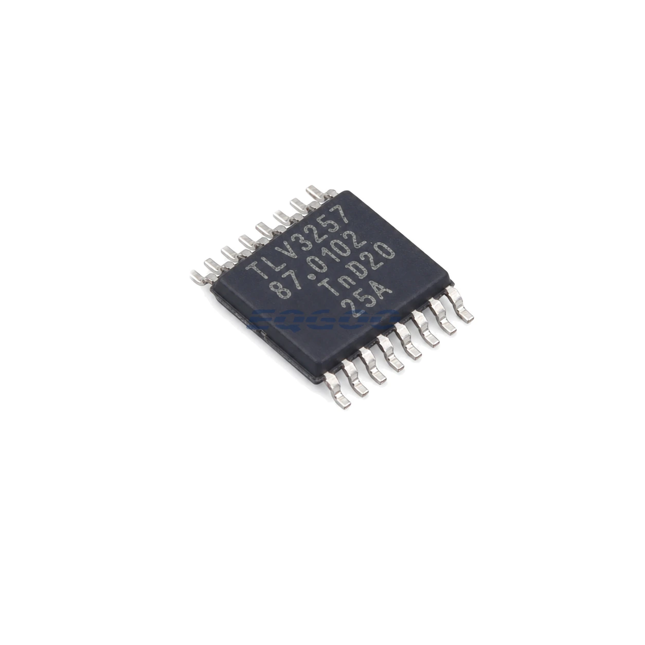
Device Overview
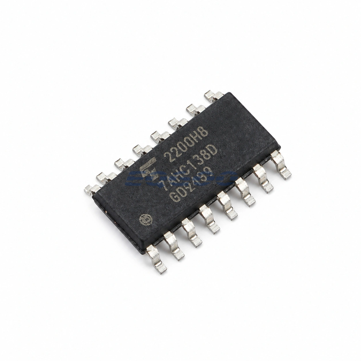
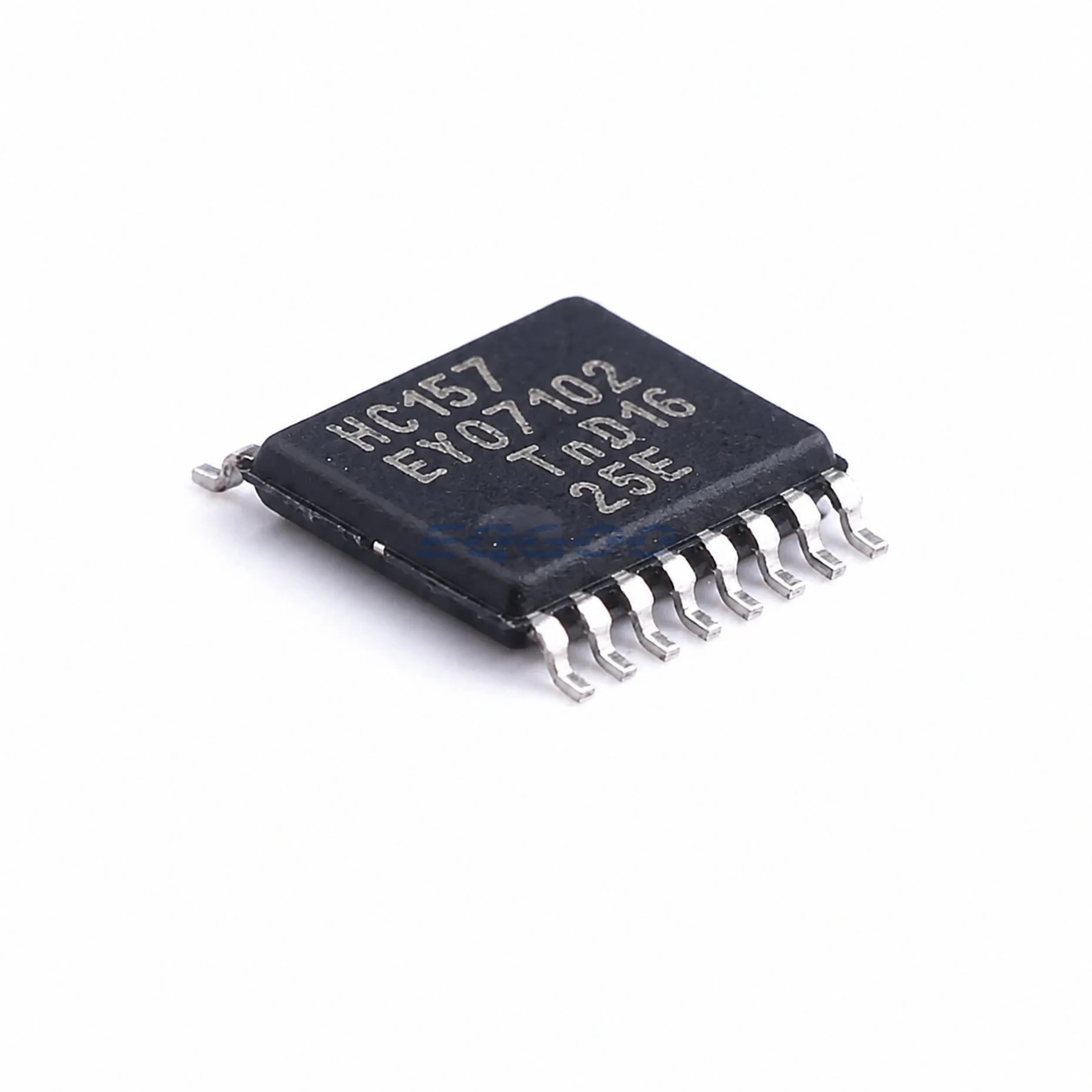
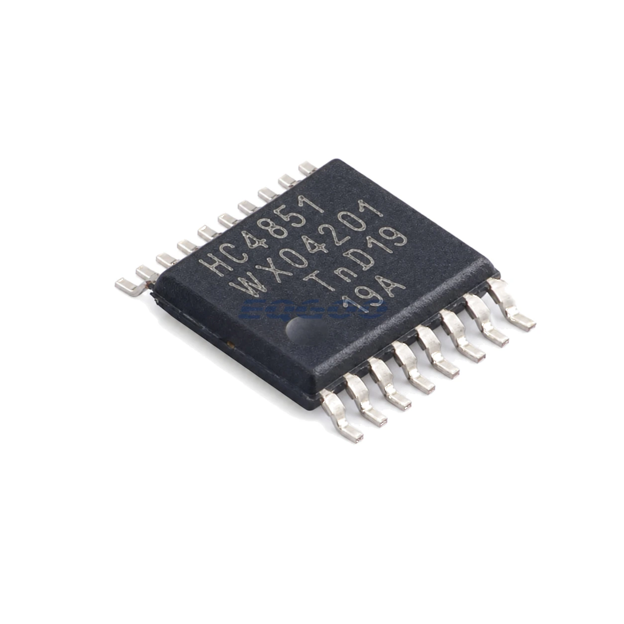
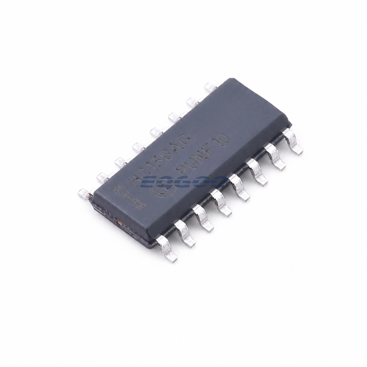
74CBTLV3257PW,118 is a Nexperia quad 1-of-2 multiplexer/demultiplexer bus switch in a TSSOP-16 package. Selection of this exact part is driven primarily by Device Function (quad 1-of-2 multiplexer/demultiplexer bus switch), Channel Topology (4 independent 1-of-2 mux/demux channels), Supply Voltage (2.3 to 3.6 V).
Selection-Critical Data
| Parameter | Confirmed Data | Why It Matters |
|---|---|---|
| Device Function | quad 1-of-2 multiplexer/demultiplexer bus switch | Defines the device function or architecture that a compatible replacement must preserve before secondary ratings are compared. |
| Channel Topology | 4 independent 1-of-2 mux/demux channels | Defines the number or arrangement of parallel signal/control paths and therefore the resources a replacement must provide. |
| Supply Voltage | 2.3 to 3.6 V | Defines compatibility with the available board power rail and required bias range. |
| On Resistance | 7 ohm (parametric class) | Affects conduction loss and heat generation under the stated current, gate-drive and temperature conditions. |
| Bandwidth | 400 MHz (-3 dB class parametric) | Defines usable signal-path bandwidth and therefore whether the device covers the intended modulation or data spectrum. |
| Propagation Delay | 0.2 ns (switch path class parametric) | Consumes part of the digital timing budget and therefore limits the maximum practical signal or control-path speed. |
| Exact Package | TSSOP-16 | Determines PCB footprint, pinout, mechanical assembly and orderable-variant compatibility. |
Logic and Interface Selection Notes
Device Function is quad 1-of-2 multiplexer/demultiplexer bus switch. Defines the device function or architecture that a compatible replacement must preserve before secondary ratings are compared. At 4 independent 1-of-2 mux/demux channels, the channel topology defines the number or arrangement of parallel signal/control paths and therefore the resources a replacement must provide.
For supply voltage, 2.3 to 3.6 V is the approved value. Defines compatibility with the available board power rail and required bias range.
Exact Package is TSSOP-16. Determines PCB footprint, pinout, mechanical assembly and orderable-variant compatibility.
7 ohm is the stated on resistance value. Affects conduction loss and heat generation under the stated current, gate-drive and temperature conditions. Technical condition: parametric class. 400 MHz is the stated bandwidth value. Defines usable signal-path bandwidth and therefore whether the device covers the intended modulation or data spectrum. Technical condition: -3 dB class parametric.
At 0.2 ns, the propagation delay consumes part of the digital timing budget and therefore limits the maximum practical signal or control-path speed. Technical condition: switch path class parametric.