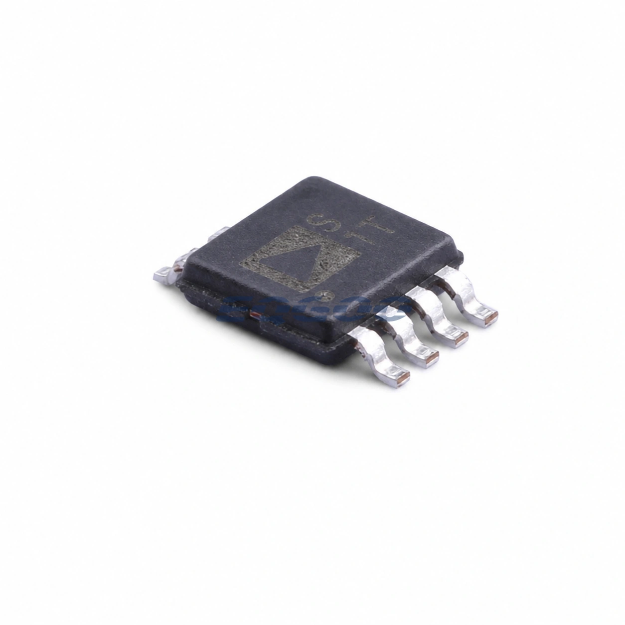
Key Selection Information
| Selection Parameter | Confirmed Information |
|---|---|
| Switch type | Absorptive SPST |
| Frequency range | DC to 4.5 GHz at -3 dB |
| Insertion loss | 0.8 dB typical at 1 GHz |
| Off isolation | 40 dB typical at 1 GHz |
| P1dB | 17 dBm typical at 1 GHz |
| Supply voltage | 1.65 V to 2.75 V |
| Control | CMOS/LVTTL |
| Package | 8-lead MSOP |
Product Overview
The ADG901BRMZ-REEL7 is the tape-and-reel 8-lead MSOP version of Analog Devices’ ADG901 wideband absorptive SPST switch. Its off-state path is terminated by internal 50 Ω shunt elements, so the disconnected RF port remains matched rather than presenting the reflective behavior of the ADG902.
The device covers DC to 4.5 GHz at its -3 dB bandwidth and is specified at only 1.65 V to 2.75 V supply voltage. At 1 GHz, Analog Devices lists 0.8 dB typical insertion loss, 40 dB typical off isolation and 17 dBm typical P1dB. Power consumption is below 1 µA because the switch uses CMOS control logic rather than a continuously biased RF core.
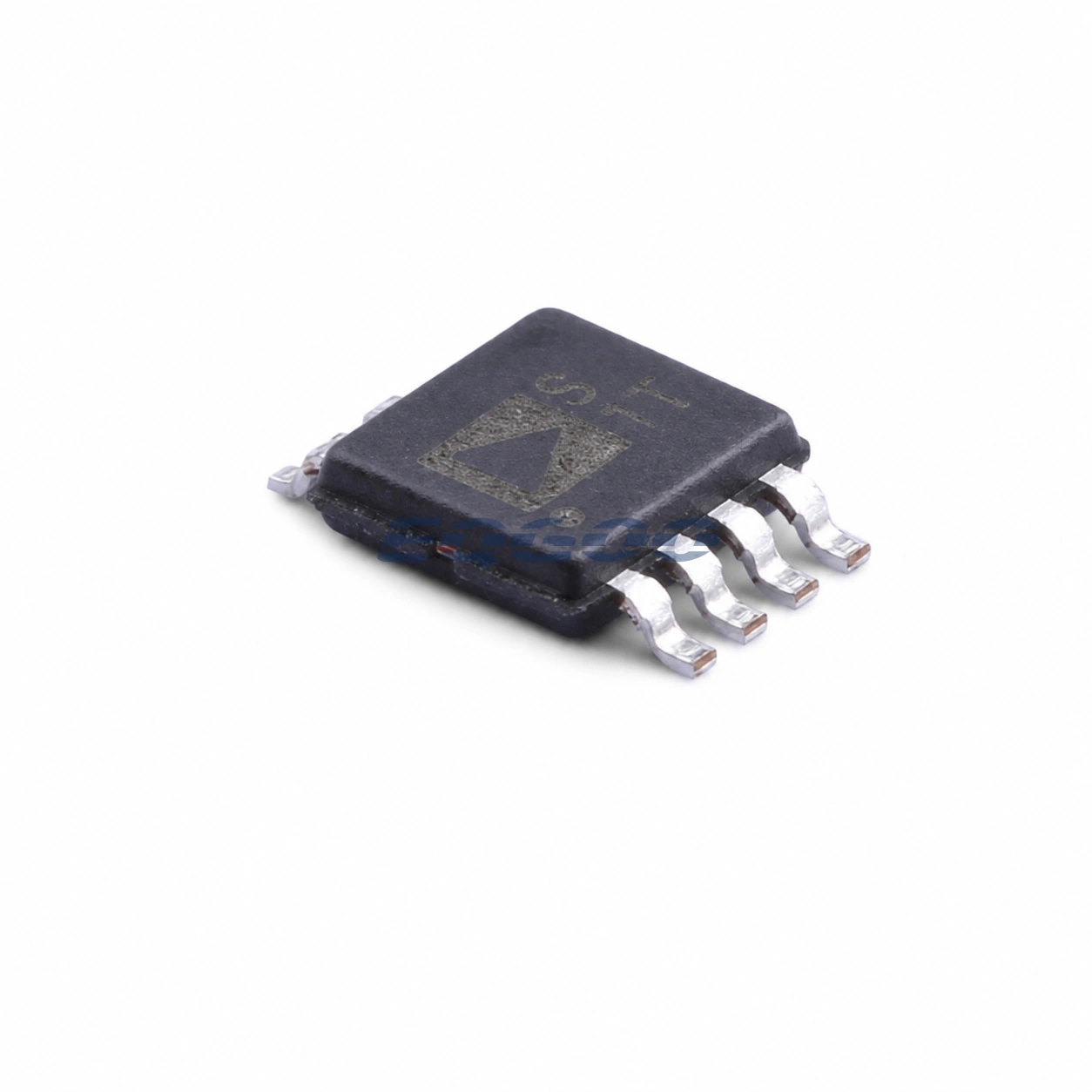
Technical Specifications
| Parameter | Confirmed Information |
|---|---|
| Topology | SPST |
| Off-state behavior | Absorptive / matched |
| Bandwidth | DC to 4.5 GHz at -3 dB |
| Insertion loss at 1 GHz | 0.8 dB typical |
| Off isolation at 1 GHz | 40 dB typical |
| P1dB at 1 GHz | 17 dBm typical |
| Supply voltage | 1.65 V to 2.75 V |
| Supply current | <1 µA |
| Control input | CMOS/LVTTL compatible |
| DC signal passing | Up to 0.5 V without a DC-blocking capacitor |
| Package | 8-lead MSOP |
| Product status | Production |
Design Considerations
The absorptive off state is useful when the source or load should remain close to 50 Ω after the switch opens. That behavior is different from the reflective ADG902, so the two parts can produce different standing-wave conditions even when insertion loss and isolation are similar.
If a DC component is present on the RF path, keep it inside the device’s documented limit. The ability to pass up to 0.5 V DC without a blocking capacitor does not imply unrestricted DC handling.
Related Engineering Resources
Quality & Verification Support
Third-party inspection or testing can be arranged according to customer requirements. Testing fees are borne by the buyer. Additional verification requirements can be discussed before shipment. After an order is placed, physical product, label, packaging, and Date Code photos may be provided where appropriate.
Request a Quote
To request a quotation, provide the manufacturer part number, required quantity, destination, target Date Code if applicable, and any testing or inspection requirements.