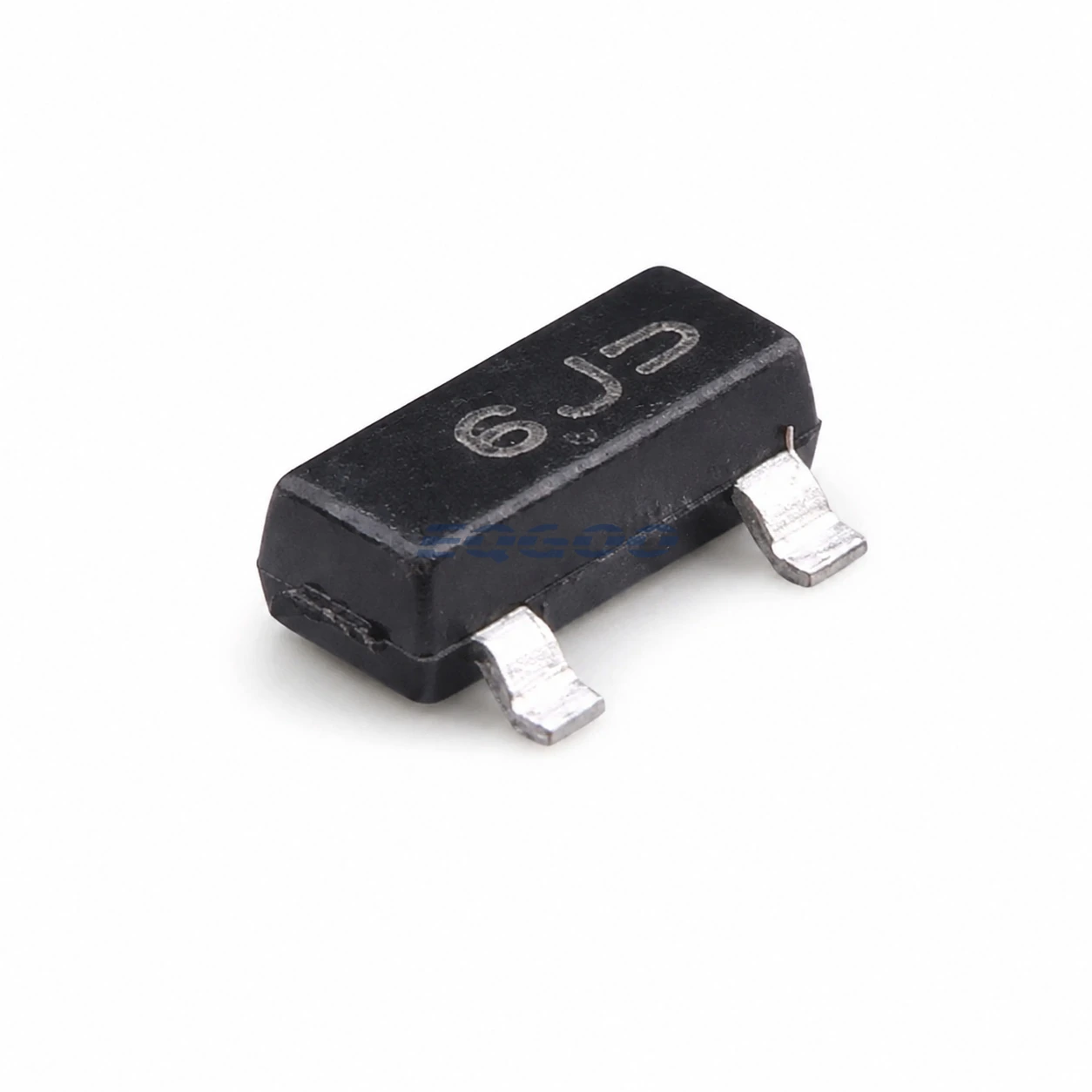
Key Selection Information
| Selection Parameter | Confirmed Information |
|---|---|
| Manufacturer | onsemi |
| Exact MPN | MMBF4391LT1G |
| Product Category | JFETs |
| Package | SOT-23 |
| Packing | 3,000 pcs/reel |
| Configuration | 1 N-channel |
| Gate-Source Cutoff Voltage (VGS(off)) | 4V |
| Gate-Source Breakdown Voltage (VGSS) | 30V |
| Power Dissipation (PD) | 225mW |
Product Overview
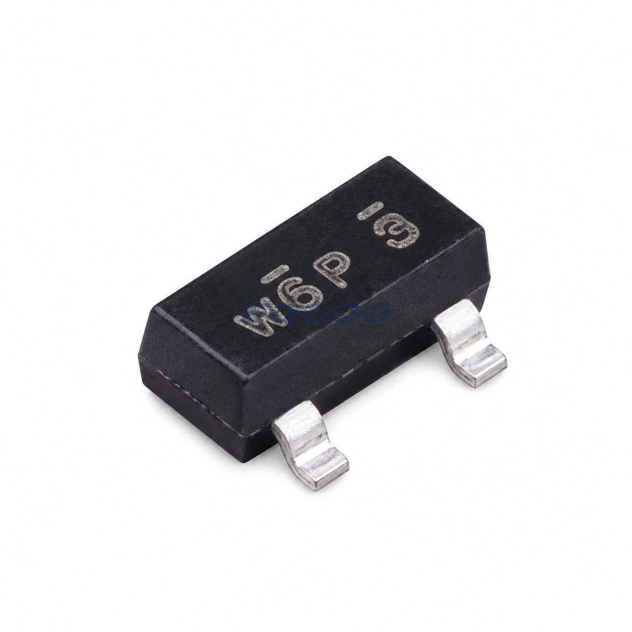
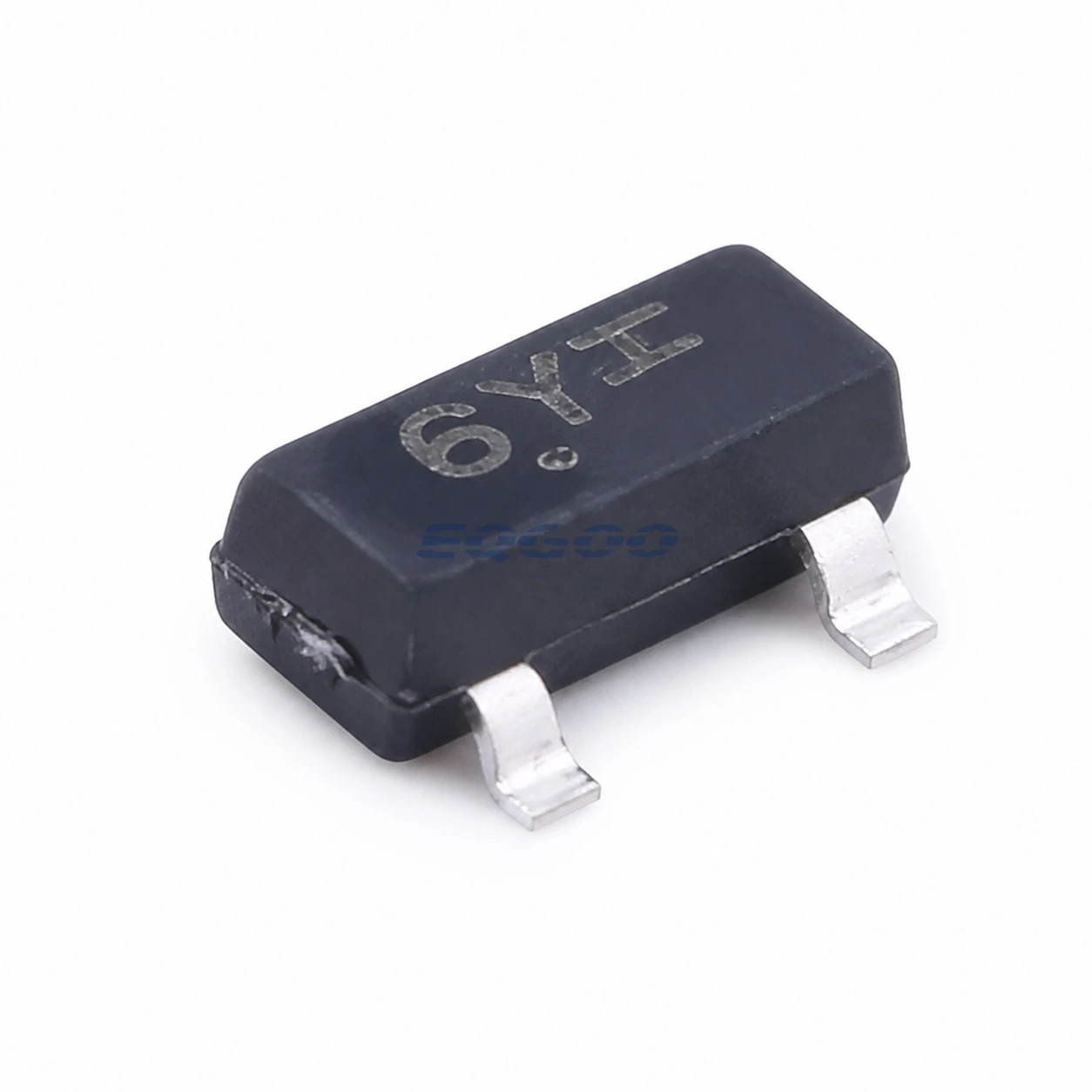
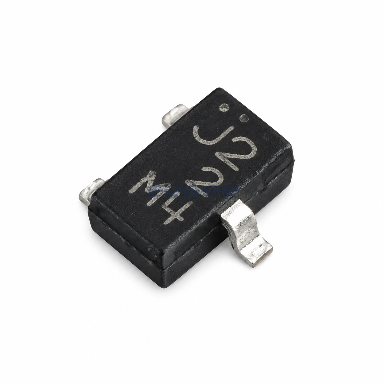
MMBF4391LT1G is a onsemi device in the JFETs category, supplied in a SOT-23 package.
Verified selection data includes Configuration: 1 N-channel, Gate-Source Cutoff Voltage (VGS(off)): 4V, Gate-Source Breakdown Voltage (VGSS): 30V, Power Dissipation (PD): 225mW.
The 50–150 mA I_{DSS} range and 30 Ω maximum resistance favor higher-current switching, but the wide spread complicates open-loop bias.
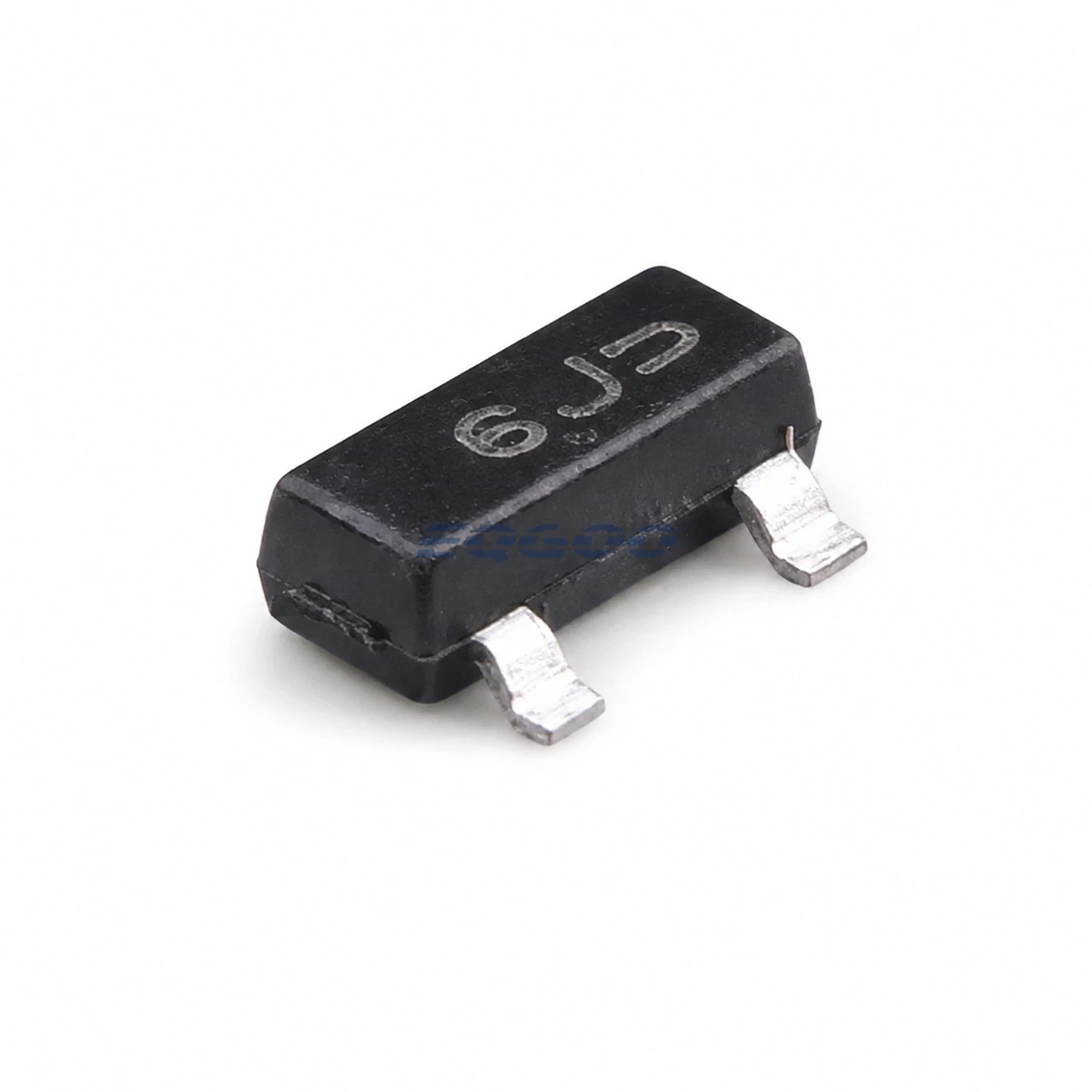
Technical Specifications
| Parameter | Verified Information |
|---|---|
| Manufacturer | onsemi |
| Exact MPN | MMBF4391LT1G |
| Functional Category | JFETs |
| Package | SOT-23 |
| Packing | 3,000 pcs/reel |
| Source Catalog ID | C153770 |
| Configuration | 1 N-channel |
| Gate-Source Cutoff Voltage (VGS(off)) | 4V |
| Gate-Source Breakdown Voltage (VGSS) | 30V |
| Power Dissipation (PD) | 225mW |
| Manufacturer Status | Active. |
Selection Notes
Highest I_{DSS} in the 4391/4392/4393 group; cutoff voltage; on-resistance; capacitance; qualification suffix.
Match channel polarity, VGS(off), breakdown voltage, current range and dissipation to the analog switch or bias point.
Manufacturer Decision-Relevant Notes
V_{DS}, V_{DG}, V_{GS} max 30 V; I_{DSS} min 50 mA, max 150 mA at V_{DS}=15 V, V_{GS}=0; V_{GS(off)} min -4.0 V, max -10 V; V_{DS(on)} max 0.4 V at I_D=12 mA; r_{DS(on)} max 30 Ω at I_D=1 mA; C_{iss} max 14 pF; C_{rss} max 3.5 pF.
Design Considerations
- Verify current and thermal margins at 150 mA; check gate-drive capability through -10 V cutoff; include 30 Ω worst-case resistance; verify all 30 V terminal ratings during switching transients.
Application Fit
Analog switching, sample-and-hold, chopper-stabilized amplifiers.
Exact Variant and Procurement Notes
SOT-23, Pb-free, 3,000/tape-and-reel; standard MMBF4391LT1G, distinct from automotive SMMBF4391LT1G.
Manufacturer Resources
Quality & Verification Support
Third-party inspection or testing can be arranged according to customer requirements. Testing fees are borne by the buyer. Additional verification requirements can be discussed before shipment. Physical product, label, packaging, and Date Code photos may be provided where appropriate.
Request a Quote
For MMBF4391LT1G quotation, provide the exact MPN, required quantity, destination, target Date Code if applicable, and any inspection or testing requirements.
For lower-current N-channel JFET switching in the same onsemi family, compare MMBF4393LT1G: its specified zero-gate drain-current range is 5–30 mA and maximum on-resistance 100 Ω, versus 50–150 mA and 30 Ω for MMBF4391LT1G under the datasheet test conditions. Recheck bias and switch resistance rather than treating these as direct replacements.