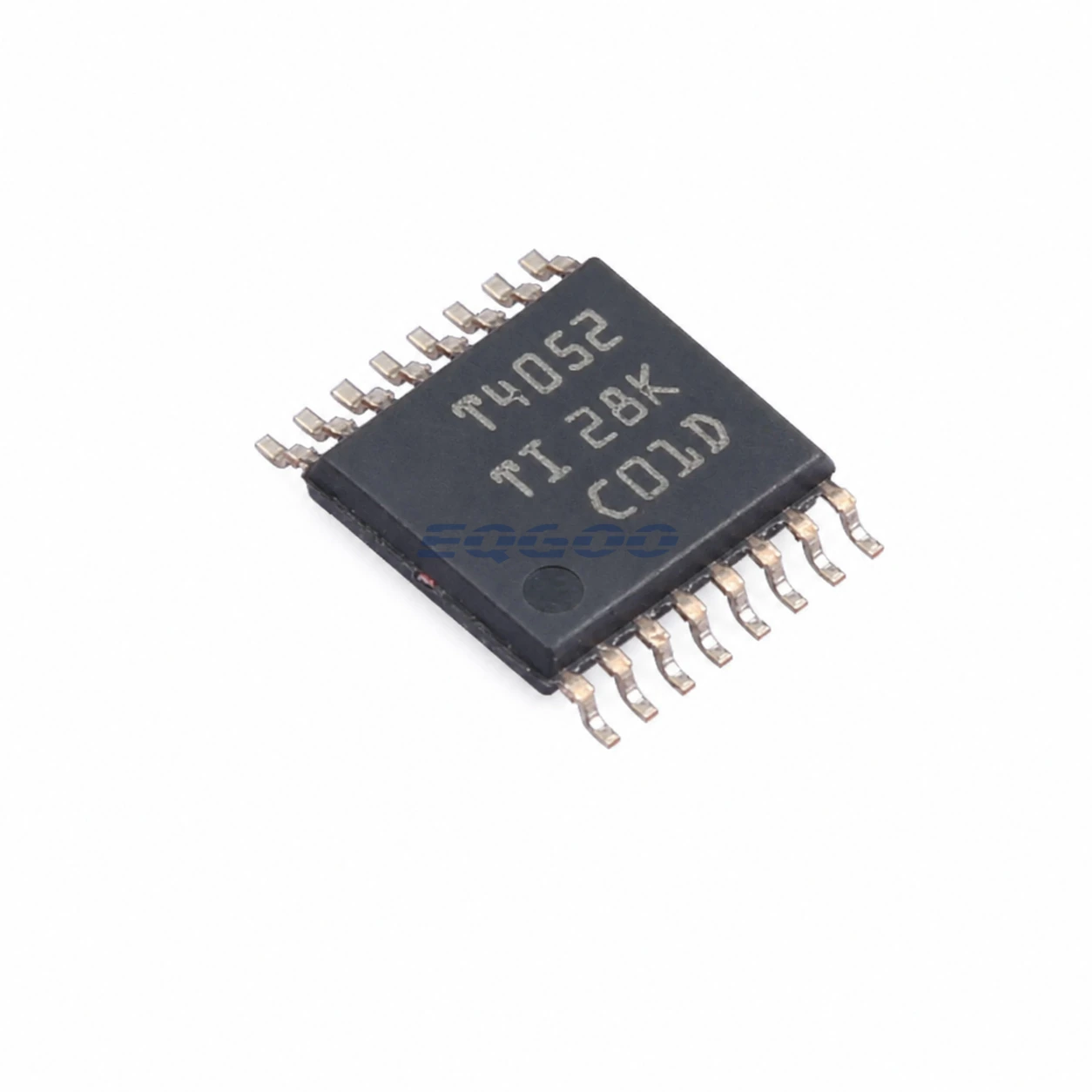

Key Selection Information
| Selection Parameter | Confirmed Information |
|---|---|
| Configuration | 2 channels, each 4:1 |
| Single Supply | 5 V to 24 V |
| Dual Supply | Up to ±12 V; asymmetric supplies supported |
| Logic | 1.8 V compatible control |
| Signal Path | Rail-to-rail from VSS to VDD, bidirectional |
| Switching | Break-before-make |
| Temperature | −55°C to +125°C family range |
| Exact Package / Packing | TSSOP (PW), 16 pins; active large-reel option |
Product Overview
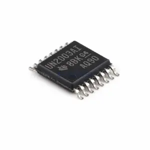
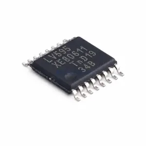
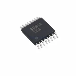
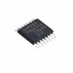
TMUX4052PWR is a modern dual 4:1 multiplexer for signal ranges that exceed 5 V. It can operate from a 24 V single supply, ±12 V dual supplies or asymmetric rails, while still accepting 1.8 V logic controls from a low-voltage processor.
Its two 4:1 banks make it suitable for differential or paired analog channels, although channel matching and source impedance should still be evaluated for precision differential measurements. It is pin-compatible in concept with industry-standard 4052-class muxes while offering modern logic thresholds.
Wide analog voltage range is the core selection value here; a low-voltage precision TMUX110x part may offer lower leakage/Ron precision but cannot replace the ±12 V signal capability.
For related devices, see HKEQGOO’s Analog Switches & Multiplexers category.
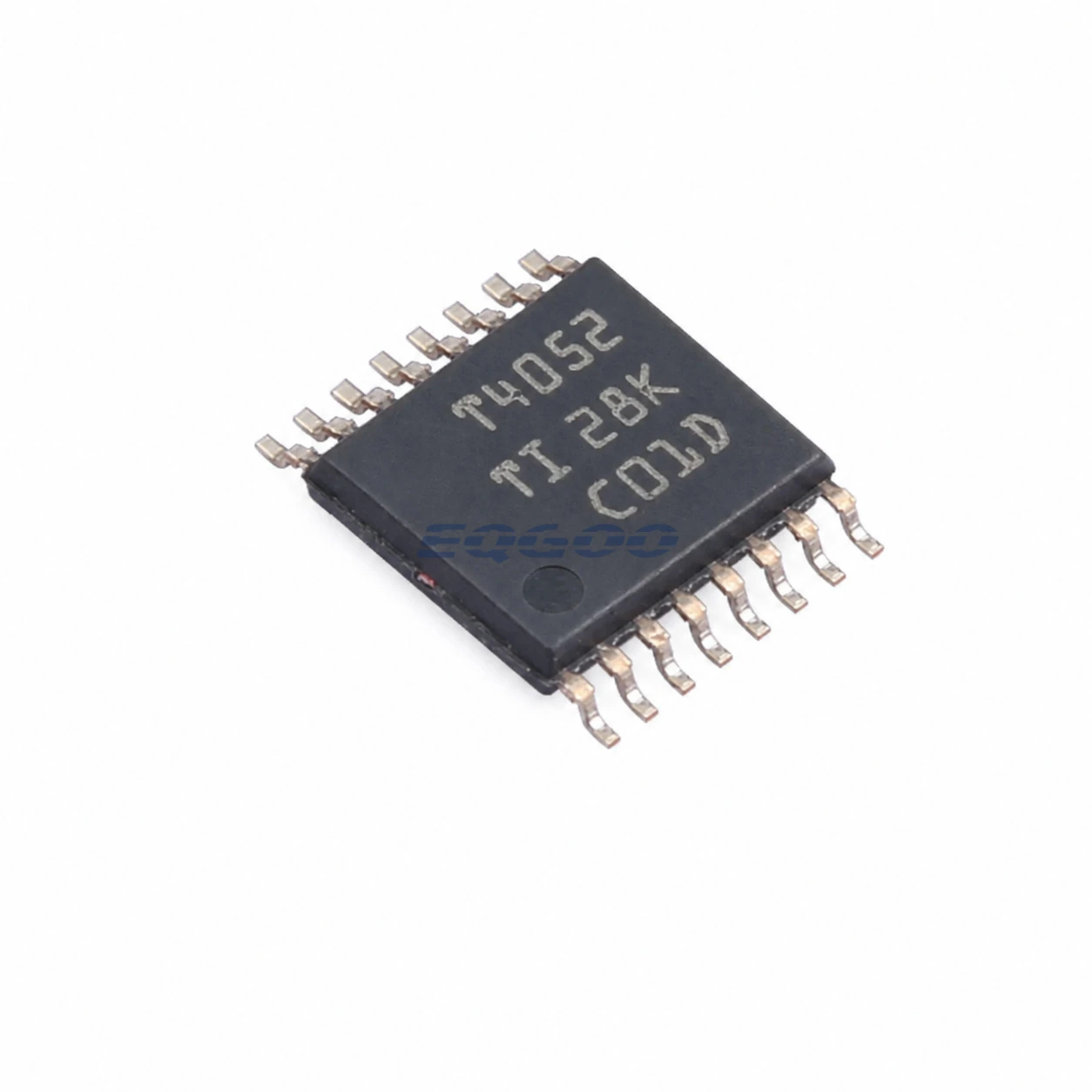
Technical Specifications
| Parameter | Verified Information |
|---|---|
| Manufacturer | Texas Instruments |
| Exact MPN | TMUX4052PWR |
| Configuration | 2 channels, each 4:1 |
| Single Supply | 5 V to 24 V |
| Dual Supply | Up to ±12 V; asymmetric supplies supported |
| Logic | 1.8 V compatible control |
| Signal Path | Rail-to-rail from VSS to VDD, bidirectional |
| Switching | Break-before-make |
| Temperature | −55°C to +125°C family range |
| Exact Package / Packing | TSSOP (PW), 16 pins; active large-reel option |
| Manufacturer Status | Active / Production |
| Part Marking | T4052 family PWR marking per TI addendum |
Functional Highlights
High analog rails and low-voltage logic can coexist
A 1.8 V MCU can select ±10 V-class industrial signals without discrete logic translation, simplifying mixed-voltage DAQ control.
Dual-bank topology suits paired signals but does not guarantee perfect pair matching
Settling and gain error still depend on each bank’s on-resistance/capacitance and the external source/load network.
Design Considerations
- Choose VDD/VSS from the actual signal extrema with switching/transient margin.
- For differential pairs, validate bank-to-bank mismatch and settling in the complete ADC/input network.
- Do not use 24 V capability as a substitute for external surge/fault protection.
Product Status and Exact Order Code
Manufacturer status: Active / Production
Texas Instruments lists TMUX4052PWR as Active / Production; TSSOP (PW), 16 pins; large tape-and-reel option; −55°C to +125°C.
Related Engineering Resources
Quality & Verification Support
Third-party inspection or testing can be arranged according to customer requirements. Testing fees are borne by the buyer. Additional verification requirements can be discussed before shipment. After an order is placed, physical product, label, packaging, and Date Code photos may be provided where appropriate.
Request a Quote
To request a quotation, provide the manufacturer part number, required quantity, destination, target Date Code if applicable, and any testing or inspection requirements.