
Key Selection Information
| Selection Parameter | Confirmed Information |
|---|---|
| Channels | 2 isolated output channels |
| Drive Strength | 4 A peak source / 6 A peak sink |
| Isolation | 5.7 kVRMS reinforced barrier |
| CMTI | Greater than 125 V/ns stated feature |
| Timing | 33 ns typical propagation delay; programmable dead time |
| Input / Output Supplies | VCCI 3 V to 18 V; VDD up to 25 V |
| Control | Fast DISABLE; two-low-side, two-high-side or half-bridge configurations |
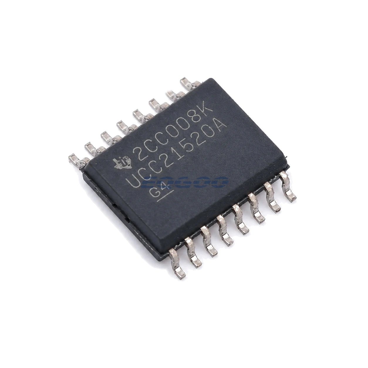
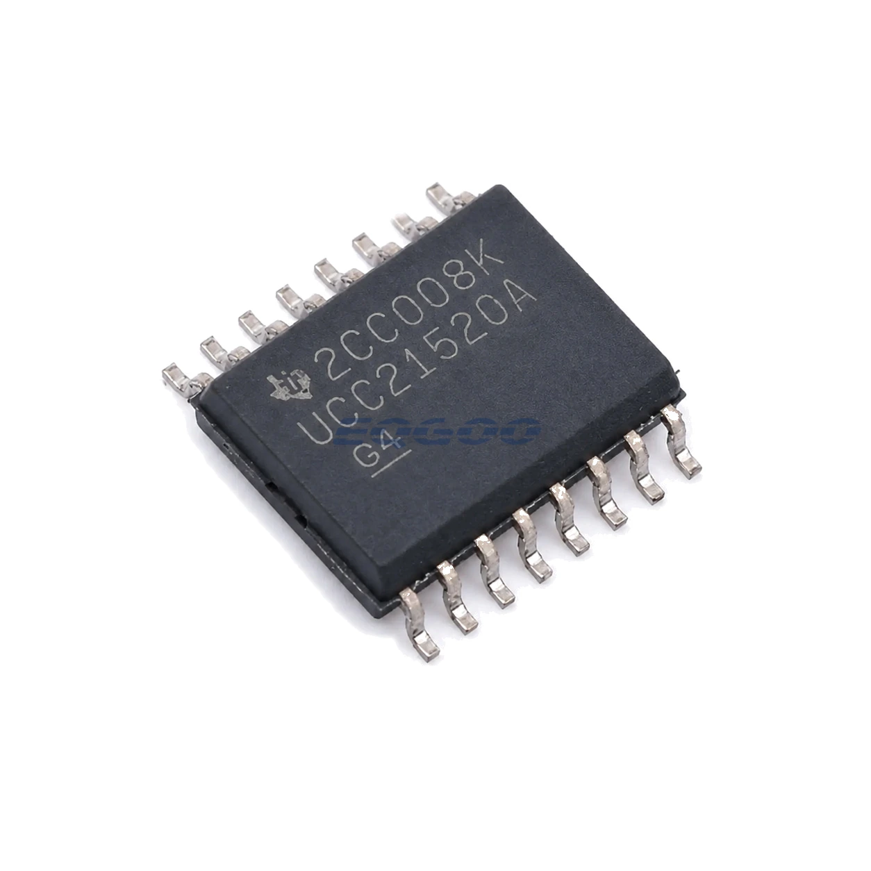
| Exact Package / Packing | SOIC (DW), 16 pins; 2000-piece large tape and reel; marking UCC21520A |
Product Overview
UCC21520ADWR is the active large-reel order code for the UCC21520A dual-channel reinforced isolated gate-driver variant. It provides two independently isolated secondary outputs with 4 A source and 6 A sink capability and can be arranged as a half bridge or as two high-/low-side drivers.
Programmable dead time is a system-level selection advantage because the same driver can be tuned for MOSFET, IGBT or SiC switching overlap requirements. The DISABLE input acts on both channels and is fast enough to participate in power sequencing and fault shutdown.
TI also lists UCC21520DWR as an active base-family order code in the same SOIC-16 reel format. Because the exact markings/order codes differ, change-controlled BOMs should preserve ADWR versus DWR rather than assuming interchangeability from the shared headline specifications.
For related devices, see HKEQGOO’s Isolators – Gate Drivers category.
Technical Specifications
| Parameter | Verified Information |
|---|---|
| Manufacturer | Texas Instruments |
| Exact MPN | UCC21520ADWR |
| Channels | 2 isolated output channels |
| Drive Strength | 4 A peak source / 6 A peak sink |
| Isolation | 5.7 kVRMS reinforced barrier |
| CMTI | Greater than 125 V/ns stated feature |
| Timing | 33 ns typical propagation delay; programmable dead time |
| Input / Output Supplies | VCCI 3 V to 18 V; VDD up to 25 V |
| Control | Fast DISABLE; two-low-side, two-high-side or half-bridge configurations |
| Exact Package / Packing | SOIC (DW), 16 pins; 2000-piece large tape and reel; marking UCC21520A |
| Manufacturer Status | Active / Production |
| Part Marking | UCC21520A |
Functional Highlights
Dead-time programming should be coordinated with the power-switch gate network
Driver dead time cannot be selected independently of propagation skew, switch turn-off tail/current, gate resistance and Miller behavior. Excess dead time increases distortion/loss; insufficient dead time risks shoot-through.
125 V/ns-class CMTI supports fast high-side transitions
High dv/dt capability is important for SiC and fast MOSFET half bridges, but PCB creepage, primary/secondary reference routing and gate-loop inductance remain just as important as the isolation IC rating.
Design Considerations
- Set dead time from measured/validated switch timing rather than copying an example value.
- Place VDD bypass capacitors and gate resistors close to each secondary output to minimize loop inductance.
- Tie DISABLE as TI recommends when unused; a floating/noisy long DISABLE route can undermine fault immunity.
Product Status and Exact Order Code
Manufacturer status: Active / Production
Texas Instruments lists UCC21520ADWR as Active / Production; SOIC (DW), 16 pins; 2000-piece large tape and reel; Level-2-260C-1 YEAR; −40°C to +125°C; marking UCC21520A.
Related Engineering Resources
Quality & Verification Support
Third-party inspection or testing can be arranged according to customer requirements. Testing fees are borne by the buyer. Additional verification requirements can be discussed before shipment. After an order is placed, physical product, label, packaging, and Date Code photos may be provided where appropriate.
Request a Quote
To request a quotation, provide the manufacturer part number, required quantity, destination, target Date Code if applicable, and any testing or inspection requirements.