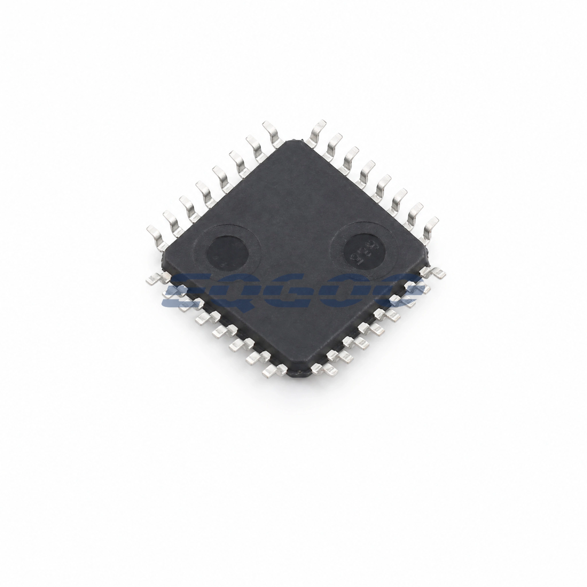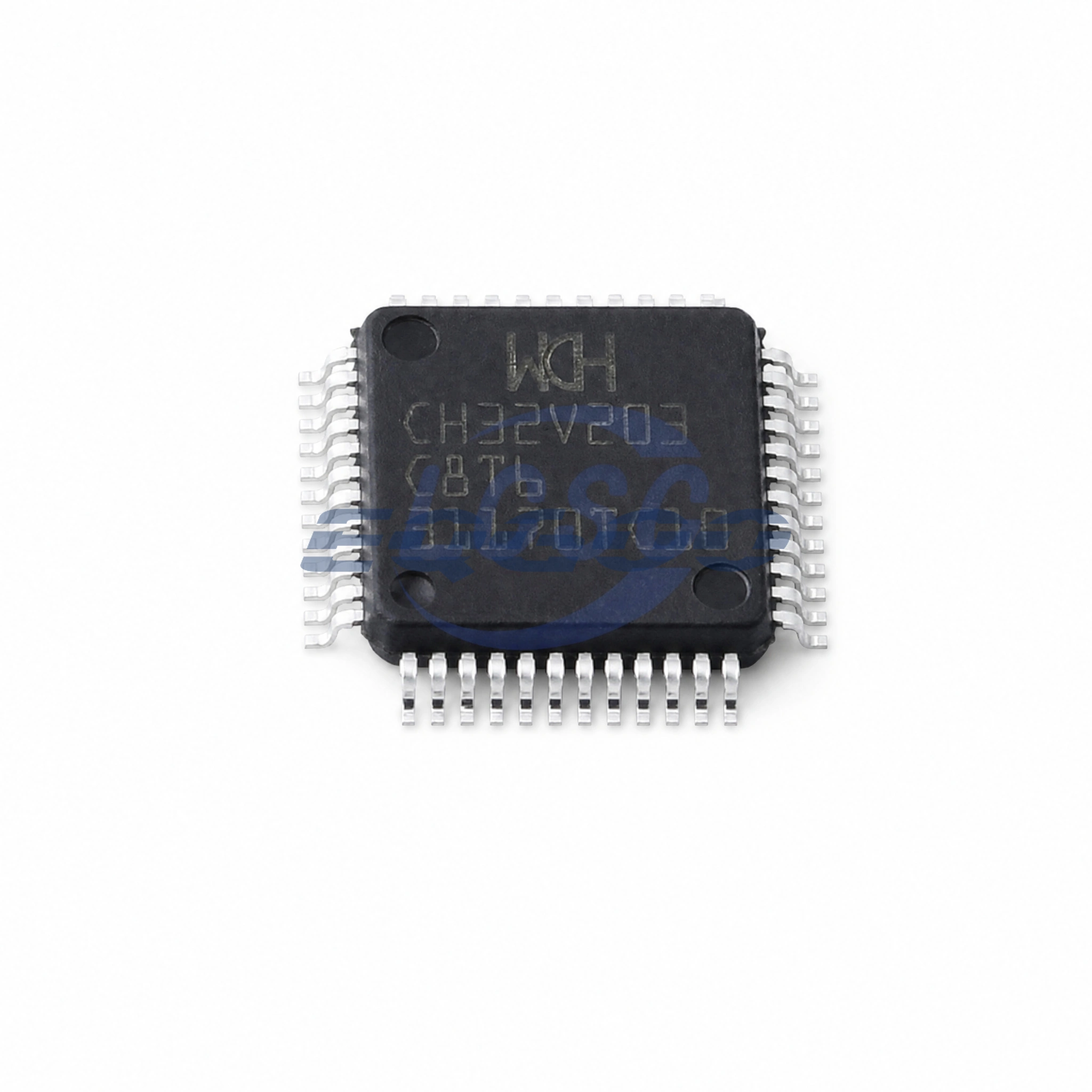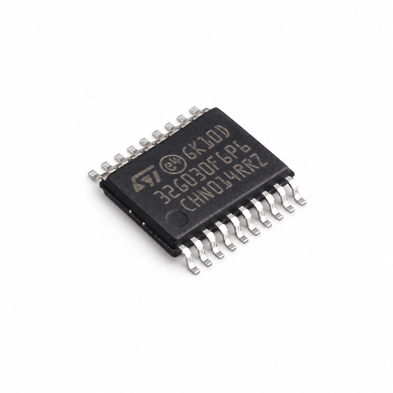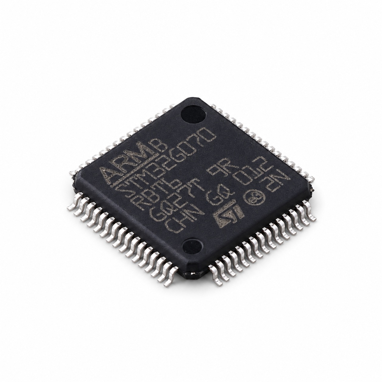
Key Selection Information
| Selection Parameter | Confirmed Information |
|---|---|
| Package | LQFP-64(10×10) |
| Supply voltage | 2V~3.6V |
| CPU Core | Arm Cortex-M0+ |
| Maximum CPU speed | 64MHz |
| Program memory | 128KB |
| Operating Temperature | -40℃~+85℃ |
| Number of I/O | 59 |
128 KB STM32G0 with a broad 64-pin I/O budget
STM32G070RBT6 pairs a 64 MHz Arm Cortex-M0+ core with 128 KB of Flash, 36 KB of SRAM and an industrial LQFP-64 package. ST lists 59 I/Os for the exact RBT6 orderable.
The communication set is a practical differentiator inside the value-line family: two SPI interfaces and four USARTs are available, together with I2C, a 12-bit ADC and the STM32G0 timer set. The part therefore targets designs that need substantially more firmware and serial-I/O headroom than the smallest STM32G0 packages.
Technical Specifications
| Parameter | Value |
|---|---|
| Package | LQFP-64(10×10) |
| Supply voltage | 2V~3.6V |
| CPU Core | Arm Cortex-M0+ |
| Maximum CPU speed | 64MHz |
| Program memory | 128KB |
| Operating Temperature | -40℃~+85℃ |
| Number of I/O | 59 |
| ADC (Bit) | 12bit |
| Program Memory Type | FLASH |
| Core Size | 32 Bit |
| Oscillator Type | Built-in+External |
Why RB/T6 is more than a larger package
The RB device combines 128 KB of Flash with the LQFP-64 pinout. Compared with compact G030 orderables, it increases both code-space headroom and the number of package-level I/Os, which directly affects how many serial, analog and control signals can coexist on the board.
Use the 59-I/O budget deliberately
- Four USARTs make multi-link serial designs more practical than on smaller G0 variants.
- Two SPI interfaces and I2C still share alternate-function pins with timers and ADC inputs, so concurrency should be proven from the exact pin map.
- 128 KB Flash and 36 KB SRAM provide more firmware/data margin, but they should still be budgeted against protocol stacks and future updates.
System fit
STM32G070RBT6 fits mainstream embedded controllers that need a larger code image and a wider set of serial and GPIO resources while retaining the Cortex-M0+ architecture. It is less compelling when the design needs CAN FD, advanced analog blocks or higher-performance DSP resources from other STM32 families.
Board-level checks
Plan the LQFP-64 alternate-function matrix before routing multiple USART/SPI links and analog inputs. Keep the 2.0 V to 3.6 V supply range in the power-tree review, and confirm that any external network interface not integrated in the device is provided by separate hardware rather than inferred from the family name.
Related Engineering Resources
- STM32G070RBT6 Datasheet (PDF) — HKEQGOO-hosted technical copy for engineering review.
- STMicroelectronics product page — official manufacturer product, lifecycle and ordering resource.
Quality & Verification Support
Third-party inspection or testing can be arranged according to customer requirements. Testing fees are borne by the buyer. Additional verification requirements can be discussed before shipment. After an order is placed, physical product, label, packaging, and Date Code photos may be provided where appropriate.
Request a Quote
To request a quotation, provide the manufacturer part number, required quantity, destination, target Date Code if applicable, and any testing or inspection requirements.