Key Selection Information
| Selection Parameter | Confirmed Information |
|---|---|
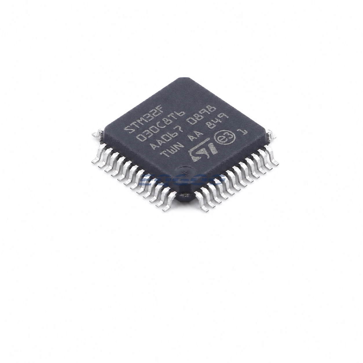
| Package | LQFP-48(7×7) |
| Supply voltage | 2.4V~3.6V |
| CPU Core | ARM Cortex-M0 |
| Maximum CPU speed | 48MHz |
| Program memory | 64KB |
| Operating Temperature | -40℃~+85℃ |
| Number of I/O | 39 |
64 KB STM32F0 with a 48-pin I/O budget
STM32F030C8T6 combines the 48 MHz Cortex-M0 STM32F030 core with 64 KB of Flash and an LQFP-48 package. ST lists the exact orderable as active, industrial grade and specified from 2.4 V to 3.6 V.
For this exact package ST lists 39 I/Os, two SPI interfaces, two USARTs and ten ADC channels. The practical advantage over smaller F030 orderables is therefore not just memory: the C8T6 also provides a wider pin budget for sensors, control outputs and serial peripherals.
Technical Specifications
| Parameter | Value |
|---|---|
| Package | LQFP-48(7×7) |
| Supply voltage | 2.4V~3.6V |
| CPU Core | ARM Cortex-M0 |
| Maximum CPU speed | 48MHz |
| Program memory | 64KB |
| Operating Temperature | -40℃~+85℃ |
| Number of I/O | 39 |
| ADC (Bit) | 12bit |
| Program Memory Type | FLASH |
| Core Size | 32 Bit |
| Oscillator Type | Built-in |
Why C8T6 is different from smaller F030 codes
The C8 density raises Flash to 64 KB, while the 48-pin T package exposes 39 I/Os. Compared with the 20-pin F4P6TR and 32-pin K6T6, this gives more room for firmware and board-level signal allocation without moving to a larger 64-pin package.
Use the package, not the family maximum, for planning
- Two SPI and two USART interfaces are available on this exact orderable according to ST’s product table.
- The 12-bit ADC is useful for mixed-signal control, but channel availability must follow the LQFP-48 pin map.
- There is no integrated CAN or USB on this F030 configuration, so designs needing those functions should select a different STM32 device rather than assume family compatibility.
Typical design fit
STM32F030C8T6 is well matched to cost-sensitive embedded controllers that need more GPIO and code space than the smallest STM32F030 packages, while keeping the simpler Cortex-M0 architecture. The 64 KB Flash and 39-I/O package are the primary reasons to choose this variant.
Board-level checks
Plan the 39 I/Os together with oscillator, debug, ADC and serial-interface alternate functions before routing the board. Treat 64 KB as a hard firmware budget, and verify that any external USB, CAN or networking function is implemented with separate hardware because it is not integrated in this device.
Related Engineering Resources
- STM32F030C8T6 Datasheet (PDF) — HKEQGOO-hosted copy of the STMicroelectronics datasheet used for technical review.
- STMicroelectronics product page — official manufacturer product, lifecycle, ordering and documentation resource.
Quality & Verification Support
Third-party inspection or testing can be arranged according to customer requirements. Testing fees are borne by the buyer. Additional verification requirements can be discussed before shipment. After an order is placed, physical product, label, packaging, and Date Code photos may be provided where appropriate.
Request a Quote
To request a quotation, provide the manufacturer part number, required quantity, destination, target Date Code if applicable, and any testing or inspection requirements.
For the smaller LQFP-32 footprint and a 32-KB Flash capacity instead of this STM32F030C8T6’s 64-KB LQFP-48 configuration, compare STM32F030K6T6 in the same STM32F030 family. Reduced Flash size and fewer available package pins change the firmware and board constraints; verify the precise ST pinout and peripheral assignment before a new design selection.