Key Selection Information
| Selection Parameter | Confirmed Information |
|---|---|
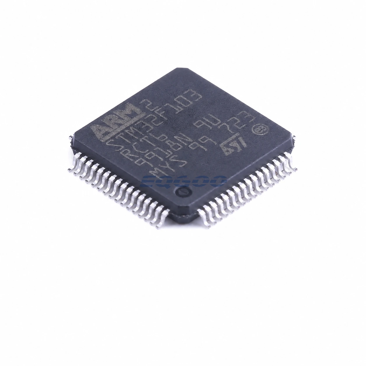
| Package | LQFP-64(10×10) |
| Supply voltage | 2V~3.6V |
| CPU Core | ARM Cortex-M3 |
| Maximum CPU speed | 72MHz |
| Program memory | 256KB |
| Operating Temperature | -40℃~+85℃ |
| Number of I/O | 51 |
High-density STM32F1 profile
STM32F103RCT6 is the 256 KB Flash, LQFP-64 member of STMicroelectronics’ high-density STM32F103 performance line. It uses a 72 MHz Arm Cortex-M3 core and ST lists the exact T6 orderable as an industrial-grade, active product. The 64-pin package exposes 51 I/Os, giving this device materially more pin and memory headroom than smaller STM32F103 packages.
The high-density F103 architecture adds three 12-bit ADCs, SDIO, three SPI interfaces, two I2S interfaces, five USARTs, USB and CAN around the Cortex-M3 core. For selection, the important point is not simply that it is an STM32F1: the RC density and 64-pin package determine how much firmware space and package-level I/O are available to the design.
Technical Specifications
| Parameter | Value |
|---|---|
| Package | LQFP-64(10×10) |
| Supply voltage | 2V~3.6V |
| CPU Core | ARM Cortex-M3 |
| Maximum CPU speed | 72MHz |
| Program memory | 256KB |
| Operating Temperature | -40℃~+85℃ |
| Number of I/O | 51 |
| DAC (Bit) | 12bit |
| ADC (Bit) | 12bit |
| Program Memory Type | FLASH |
| Core Size | 32 Bit |
| Oscillator Type | Built-in |
Why the RC / T6 combination matters
The RC device code fixes 256 KB of Flash while the T package uses LQFP-64. That combination is useful when firmware has outgrown 64 KB or 128 KB STM32F103 variants but the design still needs a 64-pin footprint rather than moving to a 100- or 144-pin package. The exact orderable is specified for the -40 °C to +85 °C industrial grade.
Interface and pin-budget decisions
- Firmware headroom: budget bootloader, protocol stacks and update margin against the exact 256 KB Flash capacity.
- Pin planning: 51 I/Os are available on this LQFP-64 orderable, but USB, CAN, SDIO, timers and serial peripherals share alternate-function pins.
- Connectivity: the device provides one CAN controller and USB; the CAN bus still requires an external physical-layer transceiver.
- Analog and control: three 12-bit ADCs and the high-density timer set make analog sampling and timer-driven control meaningful selection axes, not just family-level marketing labels.
Where this configuration fits
This orderable is a practical fit for control systems that need STM32F1 software compatibility together with 256 KB of code space, a 64-pin I/O budget, analog acquisition and both USB and CAN connectivity. It is less attractive when the project needs substantially more memory, more than 51 package I/Os, or newer security and low-power features from later STM32 generations.
Implementation checks for STM32F103RCT6
Verify the final LQFP-64 alternate-function map before committing USB, CAN, SDIO and timer channels, because the family peripheral list does not mean every signal can be used simultaneously. Keep the 2.0 V to 3.6 V supply requirement separate from any 5 V-tolerant I/O capability. If CAN is used, add the external transceiver and bus-protection network; if USB is used, budget connector, ESD, routing and clock requirements at board level.
Related Engineering Resources
- STM32F103RCT6 Datasheet (PDF) — HKEQGOO-hosted copy of the STMicroelectronics datasheet used for technical review.
- STMicroelectronics product page — official manufacturer product, lifecycle, ordering and documentation resource.
Quality & Verification Support
Third-party inspection or testing can be arranged according to customer requirements. Testing fees are borne by the buyer. Additional verification requirements can be discussed before shipment. After an order is placed, physical product, label, packaging, and Date Code photos may be provided where appropriate.
Request a Quote
To request a quotation, provide the manufacturer part number, required quantity, destination, target Date Code if applicable, and any testing or inspection requirements.