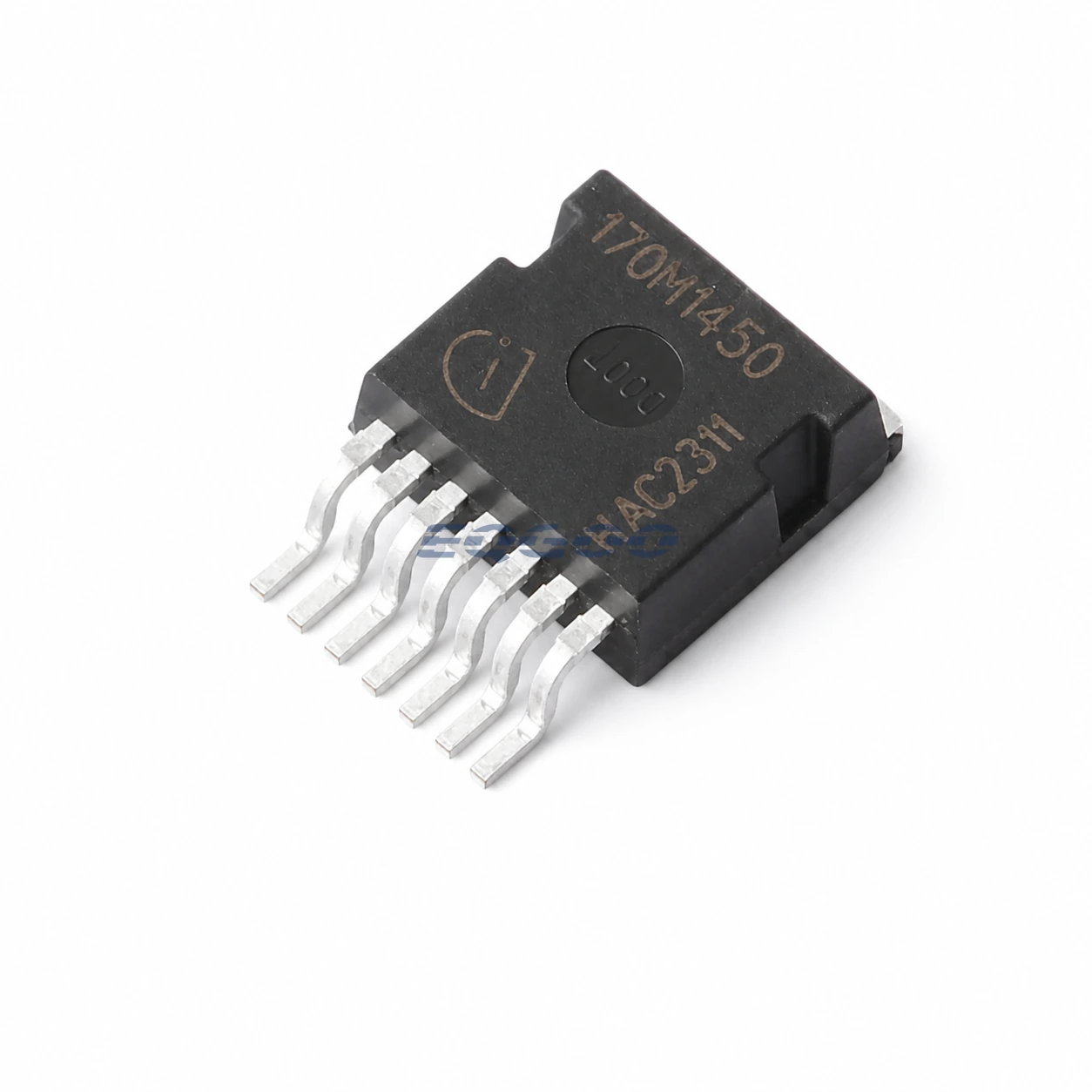
Device Overview
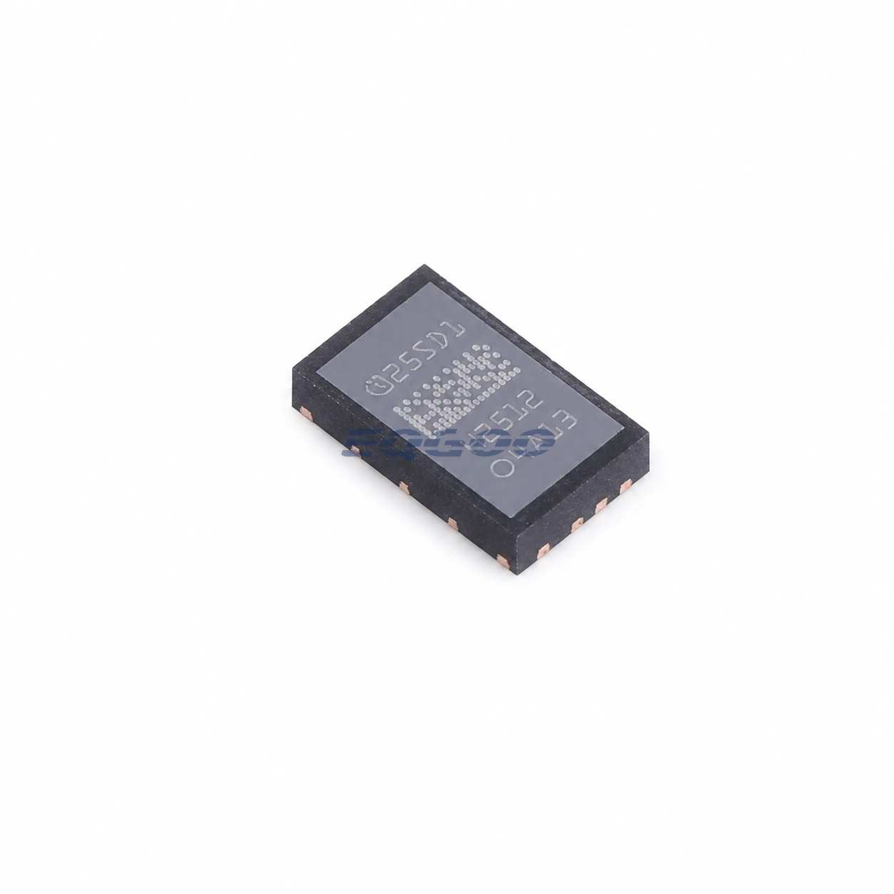
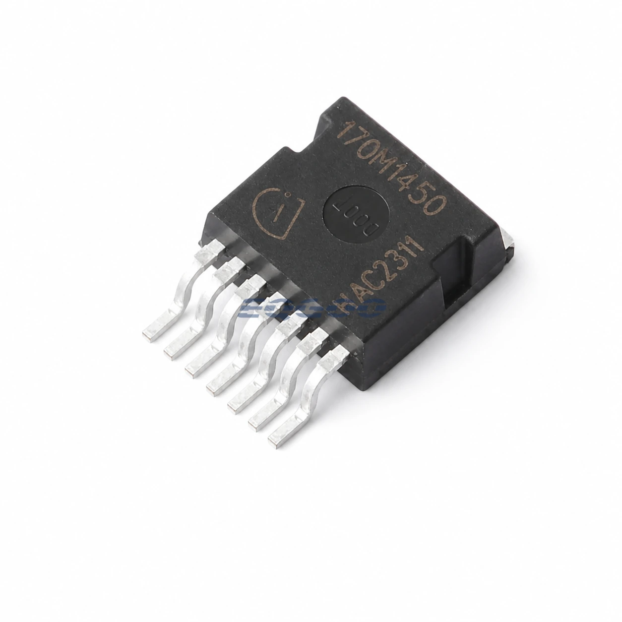
IMBF170R450M1XTMA1 is Infineon’s active and preferred CoolSiC G1 1700 V N-channel trench MOSFET in a 7-pin TO-263 package. It is intended for high-voltage switching where blocking-voltage margin, conduction loss, switching charge, thermal path, and PCB creepage must be considered together.
Key Selection Information
| Parameter | Verified Information |
|---|---|
| Manufacturer | Infineon Technologies |
| Exact OPN | IMBF170R450M1XTMA1 |
| Technology | CoolSiC G1 silicon-carbide trench MOSFET |
| Drain-source voltage | 1700 V maximum |
| Continuous drain current | 9.8 A maximum at VGS = 12 V and TC = 25 °C, limited by maximum junction temperature |
| RDS(on) | 450 mΩ typical at ID = 2 A, VGS = 12 V, Tj = 25 °C |
| Total gate charge | 11 nC |
| Gate-drain charge | 5.9 nC |
| Input capacitance | 610 pF |
| Output capacitance | 16 pF |
| Junction-temperature capability | Up to 175 °C |
| Package | TO-263-7, surface mount |
| Manufacturer lifecycle | Active and preferred |
Engineering Selection Notes
The 1700 V rating defines blocking capability, but actual design margin must include bus transients, ringing, layout inductance and the application’s insulation requirements. High-voltage SiC selection therefore cannot be reduced to VDS alone.
The 450 mΩ RDS(on) value is a typical value measured at ID = 2 A, VGS = 12 V, and Tj = 25 °C. It rises with junction temperature, so conduction-loss estimates should use the hot-device characteristic rather than applying the 25 °C typical value across the full operating range. The 9.8 A current rating uses case temperature TC = 25 °C, which is different from junction temperature Tj.
Gate threshold voltage is not an appropriate gate-drive target. Driver-voltage choice should come from the recommended operating conditions and switching-loss trade-off, while the 11 nC total gate charge and 5.9 nC gate-drain charge help estimate driver demand and switching transition behavior.
Official Engineering Resources
Alternative Candidates for Engineering Evaluation
Candidate alternatives require engineering verification before substitution. Voltage rating, RDS(on), gate charge, package, pinout, thermal behavior and qualification should be checked before use.
| MPN | Manufacturer | Package |
|---|---|---|
| NTBG028N170M1 | onsemi | D2PAK7 / TO-263-7 high-voltage |
| G3R160MT17J | Navitas | TO-263-7 |
For another 1700 V CoolSiC G1 device in TO-263-7, compare IMBF170R1K0M1XTMA1: Infineon specifies 1000 mΩ RDS(on) at Tj = 25 °C and 5.2 A maximum drain current at 25 °C, versus 450 mΩ and 9.8 A for this 450 mΩ variant. Verify thermal and switching requirements; the parts are not asserted to be drop-in equivalents.
Quality & Verification Support
Third-party inspection or testing can be arranged according to customer requirements. Testing fees are borne by the buyer. Additional verification requirements can be discussed before shipment.
Request a Quote
For IMBF170R450M1XTMA1 sourcing, provide the required quantity, destination, target Date Code if applicable, and any inspection or testing requirements.