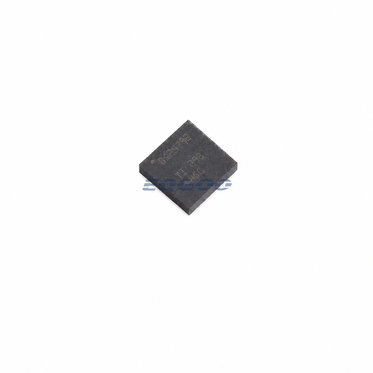

Key Selection Information
| Selection Parameter | Confirmed Information |
|---|---|
| Battery Configuration | 1 to 4 series Li-Ion / Li-Polymer cells; TI also lists LiFePO4 support |
| Charger Topology | Integrated synchronous buck-boost charger |
| Input Operating Range | 3.6 V to 24 V |
| Charge Voltage / Current | 3.0 V to 18.8 V programmable battery voltage; up to 5 A charge current |
| System Power Path | NVDC power path with programmable minimum system voltage |
| Input Selection | Dual-input selector using external bidirectional blocking NFETs |
| USB / Control | I²C, D+/D− source detection, USB OTG and integrated ADC |
| Exact Package / Packing | VQFN-HR (RQM), 29 pins, 4 mm × 4 mm; 3000-piece large tape and reel |
Product Overview
BQ25792RQMR is an integrated 1S-to-4S buck-boost battery charger designed for systems whose adapter voltage can be above or below the battery voltage. The internal switching power stage supports up to 5 A charging from a 3.6 V to 24 V input range, while the NVDC power path regulates the system rail and manages operation with weak, absent, or deeply discharged batteries.
The dual-input architecture is a key system feature. External bidirectional blocking NFETs can select between two sources while the charger manages input current and voltage limits through its power-path logic. This is useful in equipment that can receive power from more than one connector or adapter type, but the external selector FETs, source-priority policy, and fault behavior must be designed as part of the system.
BQ25792 also integrates USB-oriented functions including D+/D− source detection, USB OTG operation, input-current optimization, ADC monitoring and I²C programmability. It should not be confused with BQ25798: TI identifies MPPT/solar functionality on the BQ25798 family member, not as a BQ25792 feature.
For related devices, see HKEQGOO’s Battery Management category.
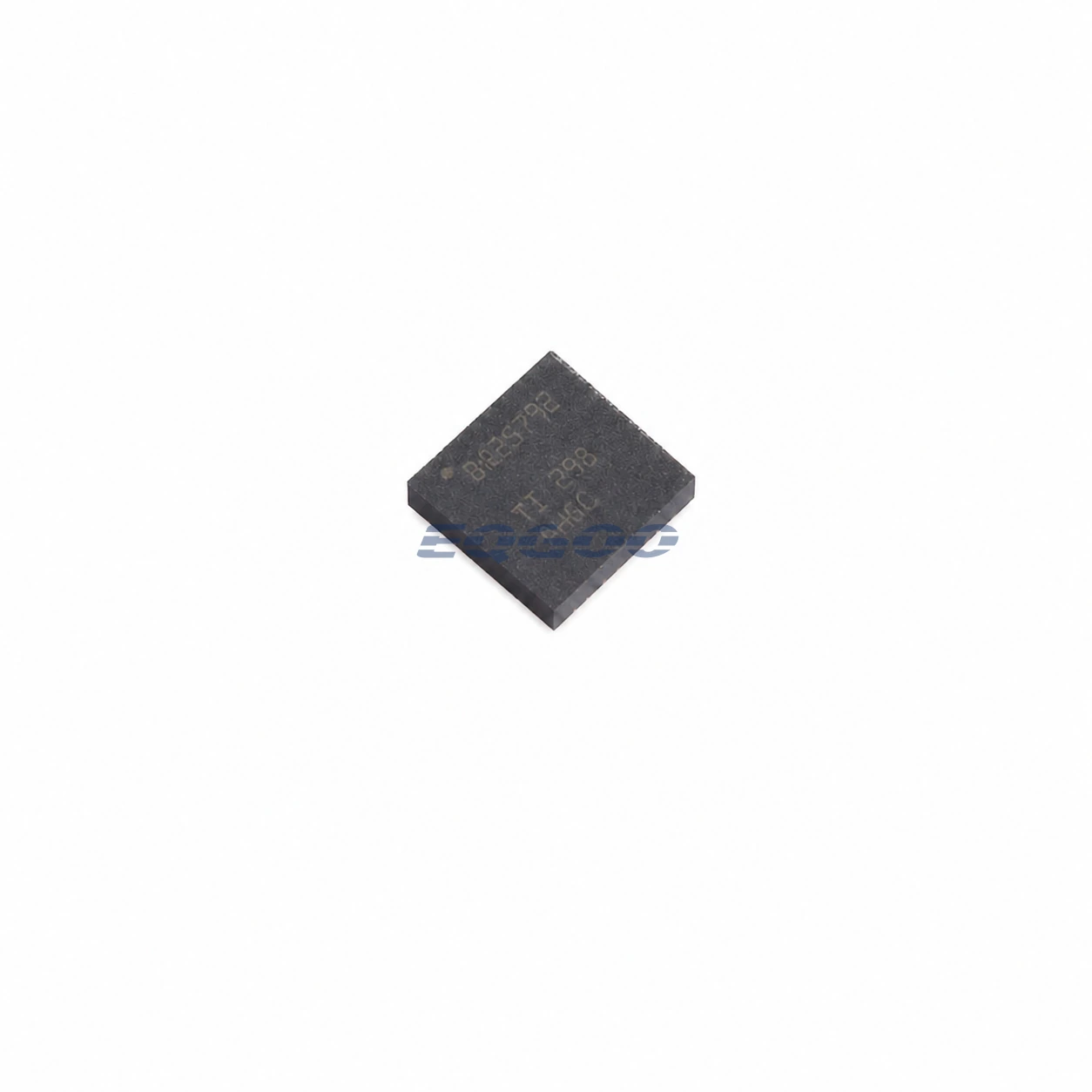
Technical Specifications
| Parameter | Verified Information |
|---|---|
| Manufacturer | Texas Instruments |
| Exact MPN | BQ25792RQMR |
| Topology | Integrated switch-mode buck-boost charger |
| Series Cells | 1 to 4 |
| Input Voltage | 3.6 V to 24 V recommended |
| Absolute Maximum Input | 30 V stated by TI product comparison data |
| Battery Regulation Range | 3.0 V to 18.8 V |
| Maximum Charge Current | 5 A |
| Switching Frequency | 750 kHz or 1.5 MHz programmable |
| Power Path | NVDC minimum-system-voltage regulation |
| Input Features | IINDPM, VINDPM, input-current optimization and dual-input selector support |
| USB Functions | D+/D− source detection and USB OTG |
| Monitoring | Integrated ADC for charger/system telemetry |
| Control Interface | I²C |
| Package | VQFN-HR (RQM), 29 pins, 4 mm × 4 mm |
| Manufacturer Status | Active / Production |
| Part Marking | BQ25792 |
Functional Highlights
Buck-boost charging removes the simple VIN-above-VBAT requirement
Because the integrated converter can operate in buck or boost regions, a source within the supported range can continue charging as the battery voltage moves relative to adapter voltage. That is useful for 1S-to-4S products that use multiple adapter classes or USB-derived sources without designing separate charger topologies.
Actual 5 A charging still depends on conversion ratio, input-current limit, source power, board thermal performance and battery conditions. The current rating should be treated as a maximum charger setting rather than a guarantee across all 3.6 V to 24 V inputs.
NVDC keeps the system rail usable during weak-battery conditions
The power path can regulate a minimum system voltage while the battery is below that level. This allows system start-up from the adapter before a deeply discharged battery has recovered. As battery and source conditions change, the charger coordinates system demand and battery charging rather than connecting the system directly to an uncontrolled battery node.
Dual-input selection requires external power-FET design
The charger can work with two input sources using external bidirectional blocking NFETs. Those devices determine conduction loss, reverse blocking, connector isolation and fault-current capability. Source-selection logic must also define what happens when both inputs are present or one source collapses.
Design Considerations
- Budget input power before assuming 5 A battery current. Low input voltage or a restrictive source-current limit can reduce charging substantially in boost operation.
- Program VSYSMIN for the downstream system rail requirement. This setting controls instant-on behavior with a depleted battery.
- Rate dual-input selector FETs for both sources. Voltage, current, reverse-blocking behavior and thermal loss belong in the charger power-path calculation.
- Treat 30 V as an absolute limit, not a normal input target. Recommended charger operation is 3.6 V to 24 V.
- Do not add solar MPPT assumptions from neighboring BQ2579x devices. BQ25792 selection should be based on its NVDC, dual-input, USB and buck-boost features.
Product Status and Exact Order Code
Manufacturer status: Active / Production
Texas Instruments lists BQ25792RQMR as an Active / Production VQFN-HR RQM 29-pin device supplied in a 3000-piece large tape-and-reel carrier, with Level-2-260C-1 YEAR MSL classification, an operating-temperature listing of −40°C to +85°C, and part marking BQ25792.
Related Engineering Resources
Quality & Verification Support
Third-party inspection or testing can be arranged according to customer requirements. Testing fees are borne by the buyer. Additional verification requirements can be discussed before shipment. After an order is placed, physical product, label, packaging, and Date Code photos may be provided where appropriate.
Request a Quote
To request a quotation, provide the manufacturer part number, required quantity, destination, target Date Code if applicable, and any testing or inspection requirements.