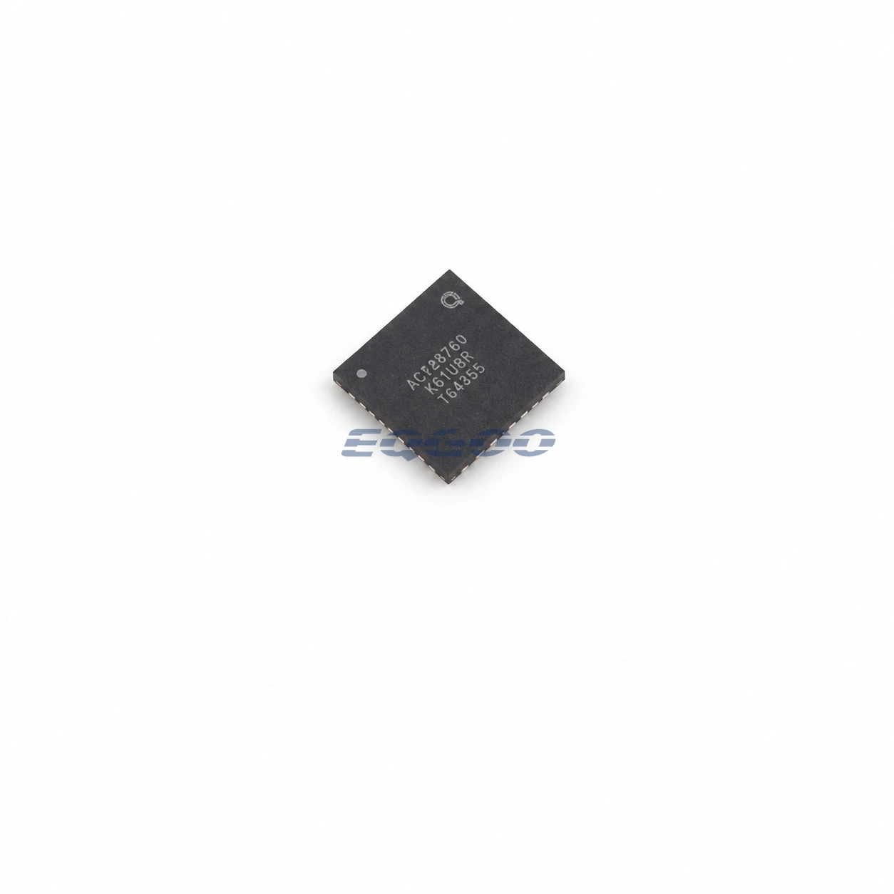
Device Overview
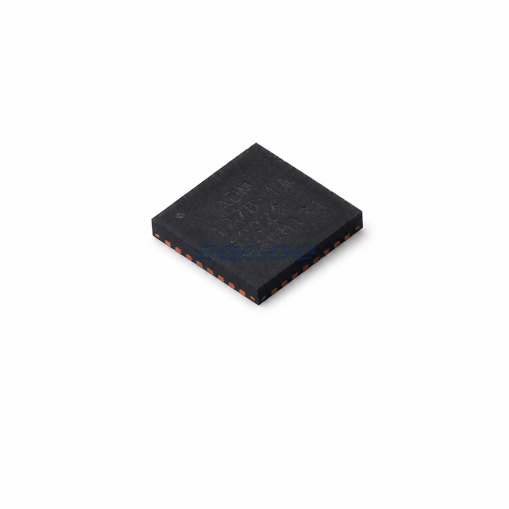
Designed as a Configurable PMIC with 7 buck converters, 6 LDOs and GPIOs, Qorvo ACT88760-101T uses the 81-pin WLCSP, 3.85 x 3.85 mm package. For substitution or design review, the strongest comparison points are Device Function (Configurable PMIC with 7 buck converters, 6 LDOs and GPIOs), Input Voltage (2.7 to 5.5 V), Output Voltage (0.5 to 3.8 V).
Selection-Critical Data
| Parameter | Confirmed Data | Why It Matters |
|---|---|---|
| Device Function | Configurable PMIC with 7 buck converters, 6 LDOs and GPIOs | Defines the device function or architecture that a compatible replacement must preserve before secondary ratings are compared. |
| Input Voltage | 2.7 to 5.5 V | Defines compatibility with the available system input rail and its operating range. |
| Output Voltage | 0.5 to 3.8 V | Defines the output/reference voltage range or setpoint that must match the target rail, battery or threshold. |
| Output Current | Buck rails up to 2-4 A depending on channel; LDO5/6 can be load switches up to 1.5 A | Defines the current-handling or drive capability that must meet the load while respecting current-path and thermal limits. |
| Regulator Resources | 7 buck converters, 6 LDO regulators | Defines how many regulated rails can be integrated into one PMIC and therefore the external regulator count the system still needs. |
| Output Capability | Buck outputs up to 4 A; dual-phase modes support higher current | Defines the current/rail capability of the integrated output stages and therefore the loads they can support without external power stages. |
| Interfaces | I2C | Defines the documented control or communication path that must remain compatible with the host and surrounding peripherals. |
| Operating Temperature | -40 to 125 degC | Defines the qualified measurement or environmental range that the design must remain within. |
| Exact Package | 81-pin WLCSP, 3.85 x 3.85 mm | Determines PCB footprint, pinout, mechanical assembly and orderable-variant compatibility. |
| Lifecycle / Procurement | Not Recommended for New Designs | The device remains a sourcing option for existing systems but should not be the preferred choice for a new platform. |
Power-Management Selection Notes
For input voltage, 2.7 to 5.5 V is the approved value. Defines compatibility with the available system input rail and its operating range. The output voltage is 0.5 to 3.8 V; this defines the output/reference voltage range or setpoint that must match the target rail, battery or threshold. At 1.5 A, the output current defines the current-handling or drive capability that must meet the load while respecting current-path and thermal limits.
At I2C, the interfaces defines the documented control or communication path that must remain compatible with the host and surrounding peripherals.
The operating temperature is -40 to 125 degC; this defines the qualified measurement or environmental range that the design must remain within.
81-pin WLCSP, 3.85 x 3.85 mm is the stated exact package value. Determines PCB footprint, pinout, mechanical assembly and orderable-variant compatibility.
For device function, Configurable PMIC with 7 buck converters, 6 LDOs and GPIOs is the approved value. Defines the device function or architecture that a compatible replacement must preserve before secondary ratings are compared. For regulator resources, 7 buck converters, 6 LDO regulators is the approved value. Defines how many regulated rails can be integrated into one PMIC and therefore the external regulator count the system still needs.
Output Capability is Buck outputs up to 4 A; dual-phase modes support higher current. Defines the current/rail capability of the integrated output stages and therefore the loads they can support without external power stages.