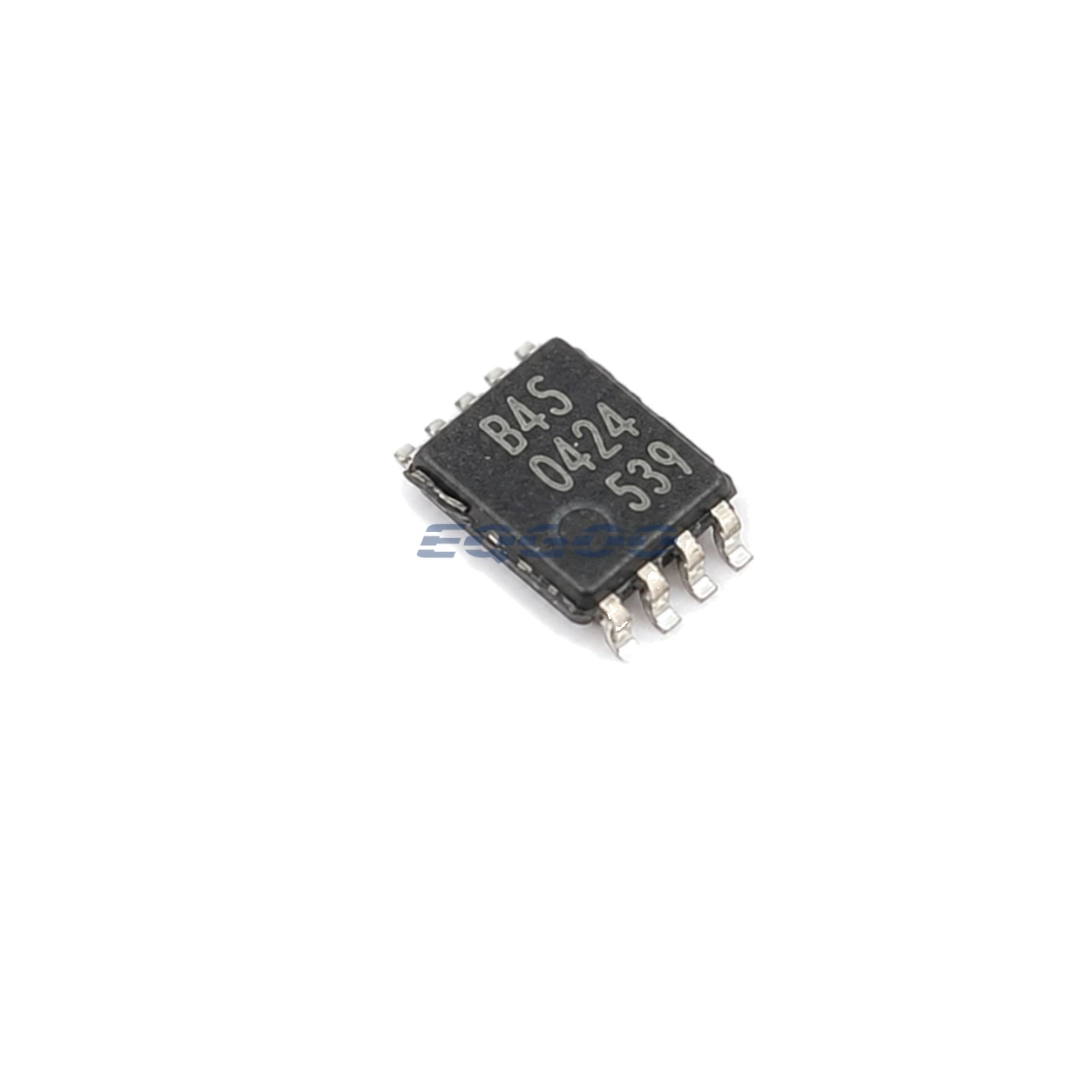
Device Overview
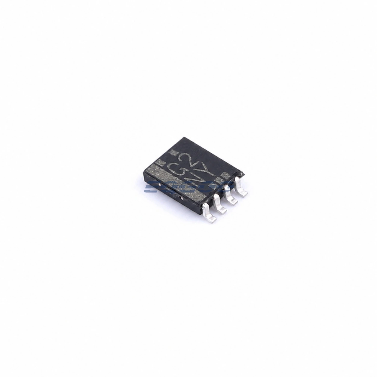
Nexperia 74AVC2T45DC-Q100H is an exact-order 2-bit dual-supply bidirectional voltage-level translator/transceiver with 3-state outputs supplied in VSSOP-8. The main engineering checks for this variant are Device Function (2-bit dual-supply bidirectional voltage-level translator/transceiver with 3-state outputs), Vcca Range (0.8 to 3.6 V), Vccb Range (0.8 to 3.6 V).
Selection-Critical Data
| Parameter | Confirmed Data | Why It Matters |
|---|---|---|
| Device Function | 2-bit dual-supply bidirectional voltage-level translator/transceiver with 3-state outputs | Defines the device function or architecture that a compatible replacement must preserve before secondary ratings are compared. |
| Vcca Range | 0.8 to 3.6 V | Defines the allowed logic-domain supply range and therefore voltage-domain compatibility for level translation between the A-side and B-side rails. |
| Vccb Range | 0.8 to 3.6 V | Defines the allowed logic-domain supply range and therefore voltage-domain compatibility for level translation between the A-side and B-side rails. |
| Maximum Data Rate | 500 Mbit/s (1.8 V to 3.3 V translation) | Defines interface throughput and timing compatibility with the source and destination devices. |
| Exact Package | VSSOP-8 | Determines PCB footprint, pinout, mechanical assembly and orderable-variant compatibility. |
| Qualification | AEC-Q100 Grade 1 | Defines a selection-critical engineering characteristic that a compatible substitute must preserve under the stated conditions. |
| Partial Power Down | I_OFF and suspend mode supported | Defines a selection-critical engineering characteristic that a compatible substitute must preserve under the stated conditions. |
Logic and Interface Selection Notes
2-bit dual-supply bidirectional voltage-level translator/transceiver with 3-state outputs is the stated device function value. Defines the device function or architecture that a compatible replacement must preserve before secondary ratings are compared.
Exact Package is VSSOP-8. Determines PCB footprint, pinout, mechanical assembly and orderable-variant compatibility.
0.8 to 3.6 V is the stated vcca range value. Defines the allowed logic-domain supply range and therefore voltage-domain compatibility for level translation between the A-side and B-side rails. For vccb range, 0.8 to 3.6 V is the approved value. Defines the allowed logic-domain supply range and therefore voltage-domain compatibility for level translation between the A-side and B-side rails.
Maximum Data Rate is 500 Mbit/s. Defines interface throughput and timing compatibility with the source and destination devices. Technical condition: 1.8 V to 3.3 V translation. At AEC-Q100 Grade 1, the qualification defines a selection-critical engineering characteristic that a compatible substitute must preserve under the stated conditions.
At I_OFF and suspend mode supported, the partial power down defines a selection-critical engineering characteristic that a compatible substitute must preserve under the stated conditions.