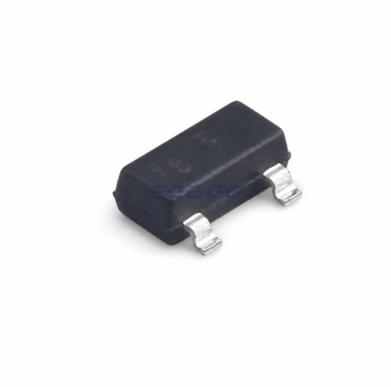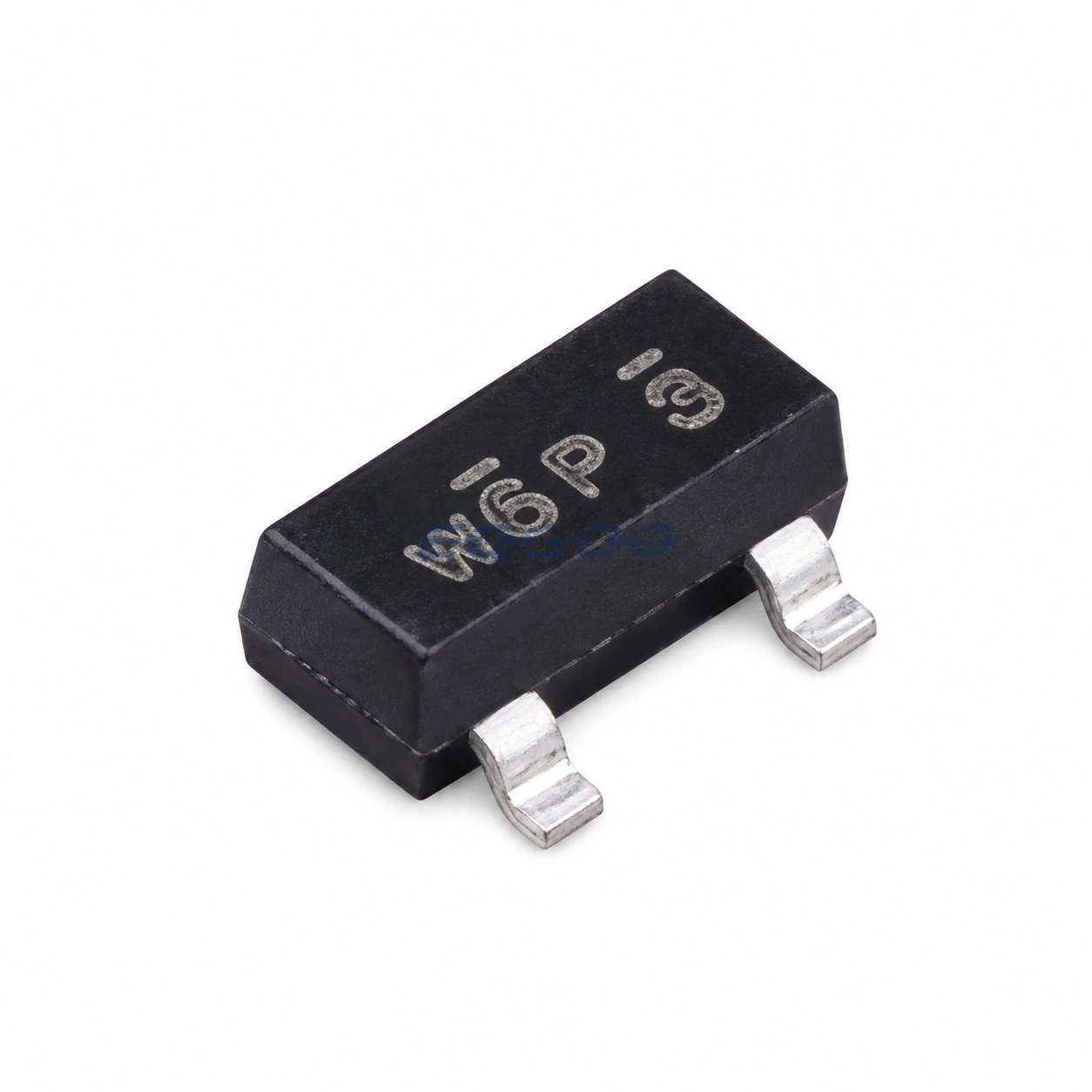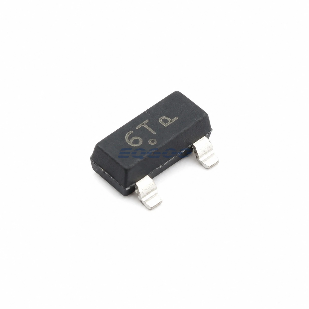
Device Overview
UF3SC065040D8S is a Qorvo JFET in a DFN8X8-4L package. For substitution or design review, the strongest comparison points are Drain-Source Voltage (650 V), Exact Package (DFN8X8-4L), Device Type (JFET).
Selection-Critical Data
| Parameter | Confirmed Data | Why It Matters |
|---|---|---|
| Drain-Source Voltage | 650 V (Maximum Ratings) | Defines the electrical voltage envelope that must cover the intended operating or stress level. |
| Exact Package | DFN8X8-4L | Determines PCB footprint, pinout, mechanical assembly and orderable-variant compatibility. |
| Device Type | Normally-off SiC cascode FET (SiC JFET + low-voltage Si MOSFET) | Defines the device function or architecture that a compatible replacement must preserve before secondary ratings are compared. |
| Continuous Drain Current | 18 A (TC < 120 C) | Defines the current-handling or drive capability that must meet the load while respecting current-path and thermal limits. |
| Pulsed Drain Current | 110 A (TC = 25 C) | Defines the current-handling or drive capability that must meet the load while respecting current-path and thermal limits. |
| RDS(on) | 42 mOhm device class at 25 degC | Affects conduction loss and heat generation under the applicable gate-drive, current and temperature conditions. |
Power-Device Selection Notes
650 V is the stated drain-source voltage value. Defines the electrical voltage envelope that must cover the intended operating or stress level. Technical condition: Maximum Ratings. For device type, JFET is the approved value. Defines the device function or architecture that a compatible replacement must preserve before secondary ratings are compared.
For exact package, DFN8X8-4L is the approved value. Determines PCB footprint, pinout, mechanical assembly and orderable-variant compatibility.
At 18 A, the continuous drain current defines the current-handling or drive capability that must meet the load while respecting current-path and thermal limits. Technical condition: TC < 120 C. The pulsed drain current is 110 A; this defines the current-handling or drive capability that must meet the load while respecting current-path and thermal limits. Technical condition: TC = 25 C.
For the same Qorvo/UnitedSiC 650 V cascode SiC FET in DFN8x8-4L with a lower typical RDS(on), compare UF3SC065030D8S with this UF3SC065040D8S. Manufacturer data for this DFN8x8-4L pair lists a 42 mΩ RDS(on) device class for UF3SC065040D8S versus about 34 mΩ typical RDS(on) at 25 °C (VGS=12 V) for UF3SC065030D8S, so conduction-loss and thermal-budget requirements differ even though both are 650 V cascode FETs in the same package family. Compare RDS(on) at your junction temperature and switching conditions; shared package naming alone does not by itself establish electrical equivalence.