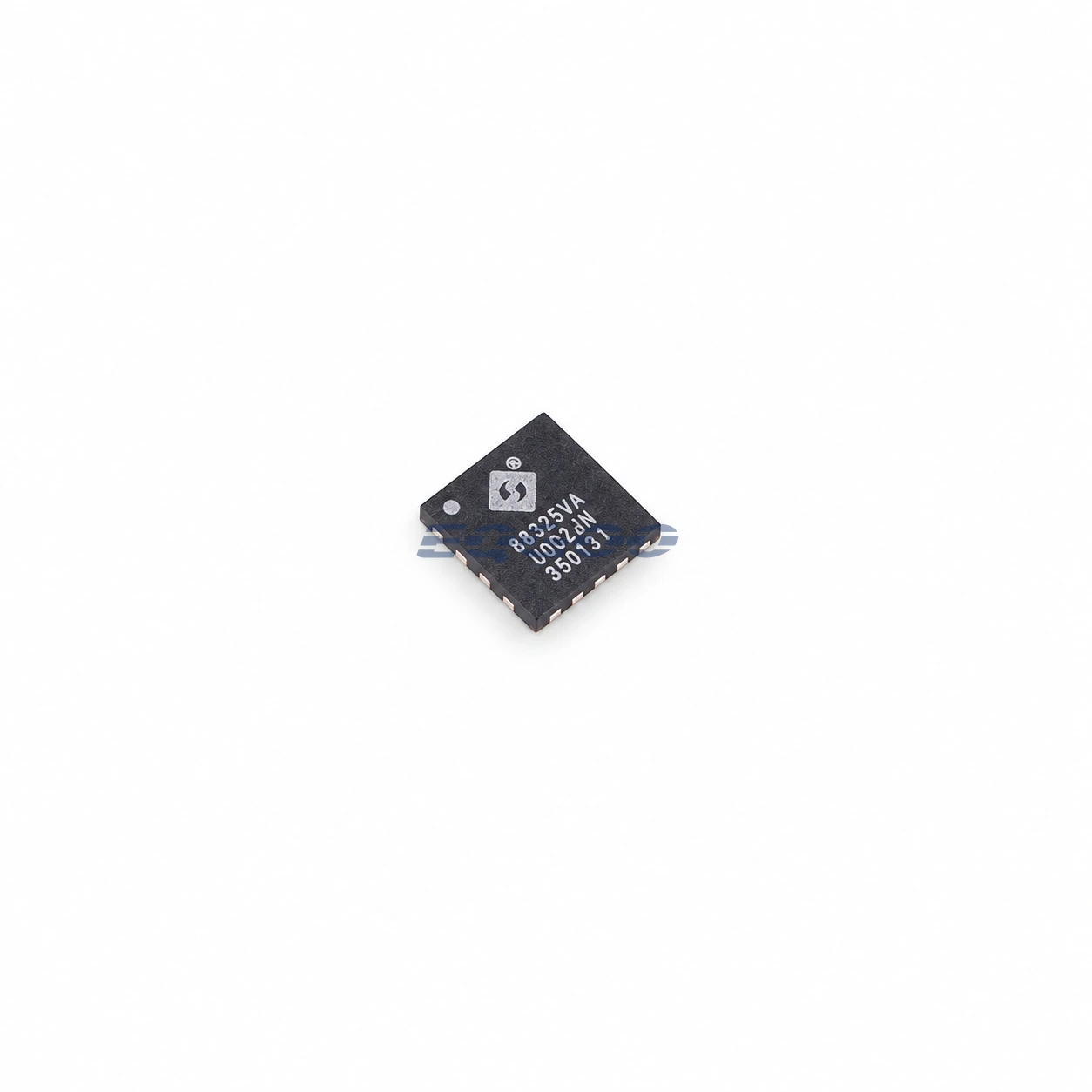
Device Overview
Designed as a Advanced PMU with 3 bucks and 2 LDOs, Qorvo ACT88325VA126-T uses the 36-ball WLCSP, 2.8 x 3.0 mm package. Selection of this exact part is driven primarily by Device Function (Advanced PMU with 3 bucks and 2 LDOs), Input Voltage (2.7 to 5.5 V), Output Current (4 A).
Selection-Critical Data
| Parameter | Confirmed Data | Why It Matters |
|---|---|---|
| Device Function | Advanced PMU with 3 bucks and 2 LDOs | Defines the device function or architecture that a compatible replacement must preserve before secondary ratings are compared. |
| Input Voltage | 2.7 to 5.5 V | Defines compatibility with the available system input rail and its operating range. |
| Output Current | 4 A (Feature block) | Defines the current-handling or drive capability that must meet the load while respecting current-path and thermal limits. |
| Exact Package | 36-ball WLCSP, 2.8 x 3.0 mm | Determines PCB footprint, pinout, mechanical assembly and orderable-variant compatibility. |
| Switching Frequency | 1.125 or 2.25 MHz | Defines the buck-converter switching-rate options and affects passive-component sizing, transient behavior and EMI. |
| Interfaces | I2C control interface; 4 configurable GPIOs | Defines the documented control or communication path that must remain compatible with the host and surrounding peripherals. |
| Lifecycle / Procurement | Qorvo page shows Production and also EOL announced 2025-06-06 / LTB 2025-12-16; ACT88321 is the recommended replacement | Because the current manufacturer page contains conflicting lifecycle signals, availability should be verified before a new commitment. |
Power-Management Selection Notes
For device function, Advanced PMU with 3 bucks and 2 LDOs is the approved value. Defines the device function or architecture that a compatible replacement must preserve before secondary ratings are compared. For input voltage, 2.7 to 5.5 V is the approved value. Defines compatibility with the available system input rail and its operating range. The output current is 4 A; this defines the current-handling or drive capability that must meet the load while respecting current-path and thermal limits. Technical condition: Feature block.
Switching Frequency is 1.125 or 2.25 MHz. Defines the operating frequency or RF band that must cover the intended signal frequencies. Technical condition: High Fsw options. The interfaces is I2C, CAN, GPIO; this defines the documented control or communication path that must remain compatible with the host and surrounding peripherals. Technical condition: Datasheet interfaces/features.
At 36-ball WLCSP, 2.8 x 3.0 mm, the exact package determines PCB footprint, pinout, mechanical assembly and orderable-variant compatibility.