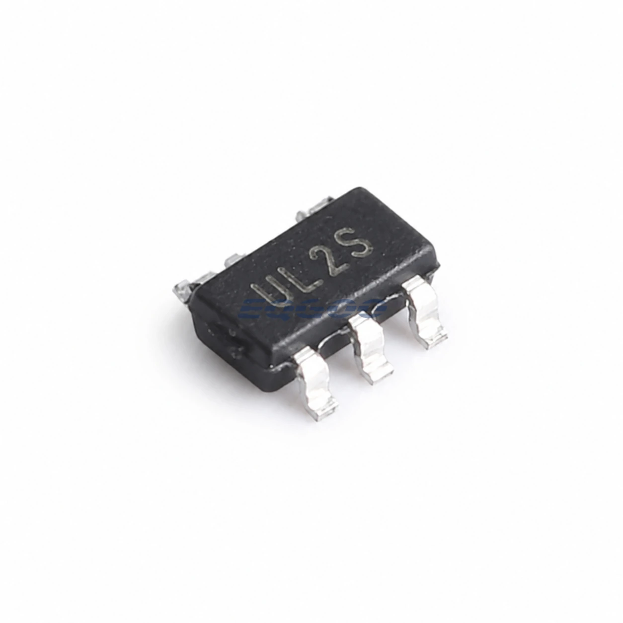
Device Overview
Microchip Technology MCP1824T-0802E/OT is an exact-order 300 mA low-voltage low-quiescent-current LDO regulator supplied in SOT-23-5. Selection of this exact part is driven primarily by Device Function (300 mA low-voltage low-quiescent-current LDO regulator), Input Voltage (2.1 to 6.0 V), Output Current (300 mA).
Selection-Critical Data
| Parameter | Confirmed Data | Why It Matters |
|---|---|---|
| Device Function | 300 mA low-voltage low-quiescent-current LDO regulator | Defines the device function or architecture that a compatible replacement must preserve before secondary ratings are compared. |
| Input Voltage | 2.1 to 6.0 V | Defines compatibility with the available system input rail and its operating range. |
| Output Current | 300 mA | Defines the current-handling or drive capability that must meet the load while respecting current-path and thermal limits. |
| Dropout Voltage | 200 mV (typical at 300 mA) | Defines the electrical voltage envelope that must cover the intended operating or stress level. |
| Quiescent Current | 220 uA (maximum) | Defines DC power and thermal burden on the bias or supply rail. |
| Exact Package | SOT-23-5 | Determines PCB footprint, pinout, mechanical assembly and orderable-variant compatibility. |
| Features | shutdown input and power-good output (MCP1824 variant) | Defines a selection-critical engineering characteristic that a compatible substitute must preserve under the stated conditions. |
Power-Management Selection Notes
Device Function is 300 mA low-voltage low-quiescent-current LDO regulator. Defines the device function or architecture that a compatible replacement must preserve before secondary ratings are compared. Input Voltage is 2.1 to 6.0 V. Defines compatibility with the available system input rail and its operating range. The output current is 300 mA; this defines the current-handling or drive capability that must meet the load while respecting current-path and thermal limits.
At 200 mV, the dropout voltage defines the electrical voltage envelope that must cover the intended operating or stress level. Technical condition: typical at 300 mA.
For quiescent current, 220 uA is the approved value. Defines DC power and thermal burden on the bias or supply rail. Technical condition: maximum.
At SOT-23-5, the exact package determines PCB footprint, pinout, mechanical assembly and orderable-variant compatibility.
For features, shutdown input and power-good output is the approved value. Defines a selection-critical engineering characteristic that a compatible substitute must preserve under the stated conditions. Technical condition: MCP1824 variant.