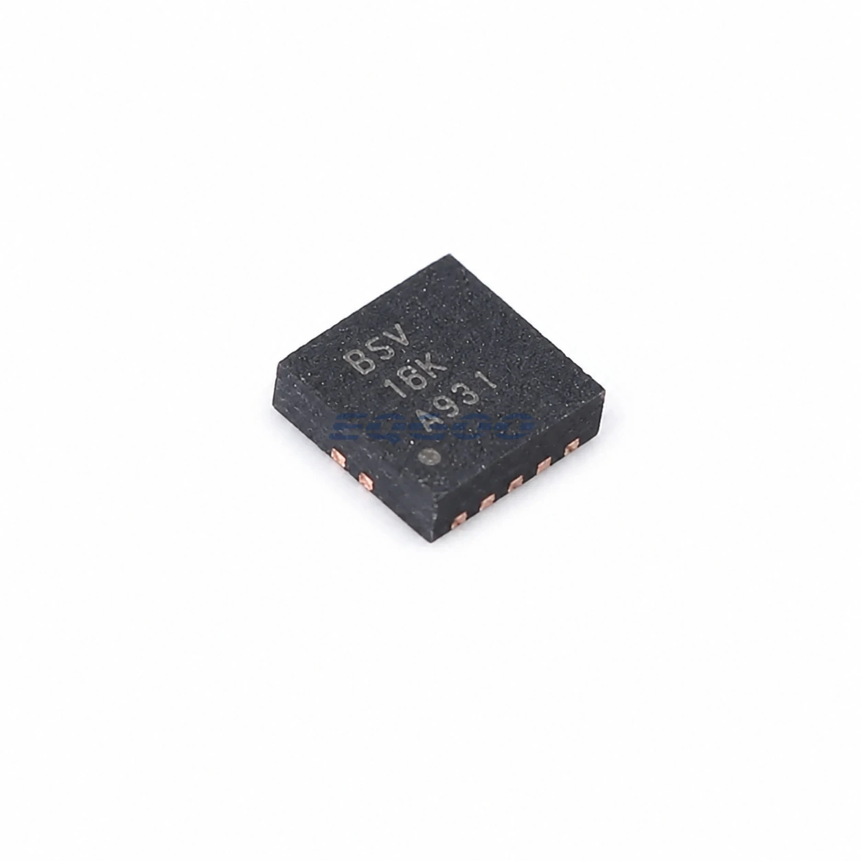

Key Selection Information
| Selection Parameter | Confirmed Information |
|---|---|
| Function | Precision voltage-to-current converter/transmitter |
| Output Ranges | 0–20 mA, 4–20 mA, 5–25 mA; up to 32 mA source |
| Transfer Setting | Single RSET sets current ratio |
| Accuracy / Linearity | 0.015% accuracy; 0.002% nonlinearity stated features |
| Supply | 7 V to 44 V |
| Auxiliary | 3 V to 15 V adjustable regulator, EF and OD |
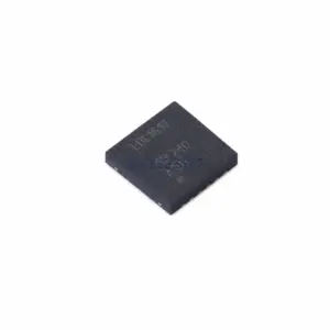
| Package | VSON (DRC), 10 pins, 3 mm × 3 mm |
| Exact Packing | 3000-piece large tape and reel; marking BSV |
Product Overview
XTR111AIDRCR puts the same precision voltage-to-current architecture into a 3 mm × 3 mm leadless VSON package. It is selected when analog-output density matters enough to justify a smaller footprint and a leadless assembly process.
The DRC package does not remove the external P-MOSFET: the transistor still carries output compliance/power dissipation while the XTR111 regulates the current according to VIN and RSET. PCB area saved at the controller must therefore be considered together with the required external pass-device area and thermal path.
Compared with DGQR/DGQT, DRCR changes footprint and assembly, not the core transfer. The 3000-piece reel and BSV marking are part of the exact procurement identity.
For related devices, see HKEQGOO’s ADCs/DACs – Special Purpose category.
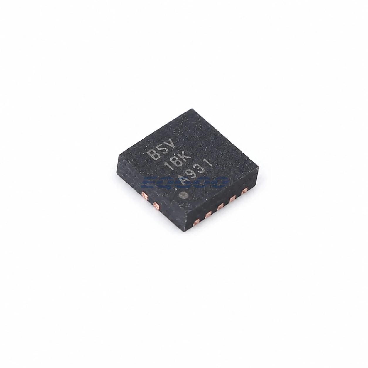
Technical Specifications
| Parameter | Verified Information |
|---|---|
| Manufacturer | Texas Instruments |
| Exact MPN | XTR111AIDRCR |
| Function | Precision voltage-to-current converter/transmitter |
| Output Ranges | 0–20 mA, 4–20 mA, 5–25 mA; up to 32 mA source |
| Transfer Setting | Single RSET sets current ratio |
| Accuracy / Linearity | 0.015% accuracy; 0.002% nonlinearity stated features |
| Supply | 7 V to 44 V |
| Auxiliary | 3 V to 15 V adjustable regulator, EF and OD |
| Package | VSON (DRC), 10 pins, 3 mm × 3 mm |
| Exact Packing | 3000-piece large tape and reel; marking BSV |
| Manufacturer Status | Active / Production |
| Part Marking | BSV |
Functional Highlights
3×3 VSON saves controller area but increases assembly sensitivity
Exposed/leadless pads demand correct stencil, solder coverage and inspection. This can be worthwhile in dense I/O modules but should be treated as a manufacturing change versus HVSSOP.
Overall channel area is not just the IC footprint
The external PMOS, current-limit components and thermal copper may dominate channel area at high compliance voltage, so VSON selection should be based on the complete output-stage layout.
Design Considerations
- Use TI’s DRC land pattern and exposed-pad guidance; do not reuse the DGQ footprint.
- Place RSET away from hot PMOS copper if its tempco/thermal gradient can affect current accuracy.
- Check PMOS SOA and VSON thermal environment together for maximum loop voltage/current.
Product Status and Exact Order Code
Manufacturer status: Active / Production
Texas Instruments lists XTR111AIDRCR as Active / Production; VSON (DRC), 10 pins, 3 mm × 3 mm; 3000-piece large tape and reel; Level-2-260C-1 YEAR; −40°C to +125°C; marking BSV.
Related Engineering Resources
Quality & Verification Support
Third-party inspection or testing can be arranged according to customer requirements. Testing fees are borne by the buyer. Additional verification requirements can be discussed before shipment. After an order is placed, physical product, label, packaging, and Date Code photos may be provided where appropriate.
Request a Quote
To request a quotation, provide the manufacturer part number, required quantity, destination, target Date Code if applicable, and any testing or inspection requirements.