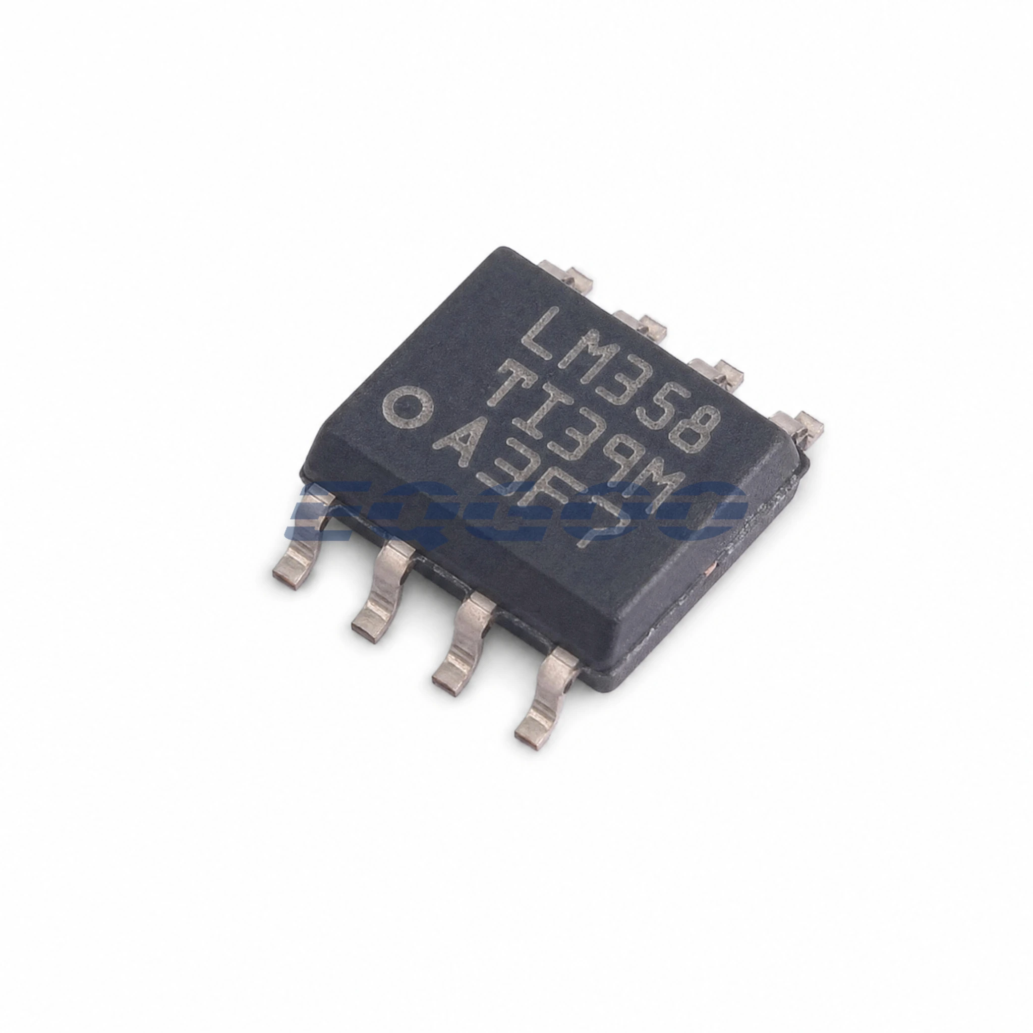
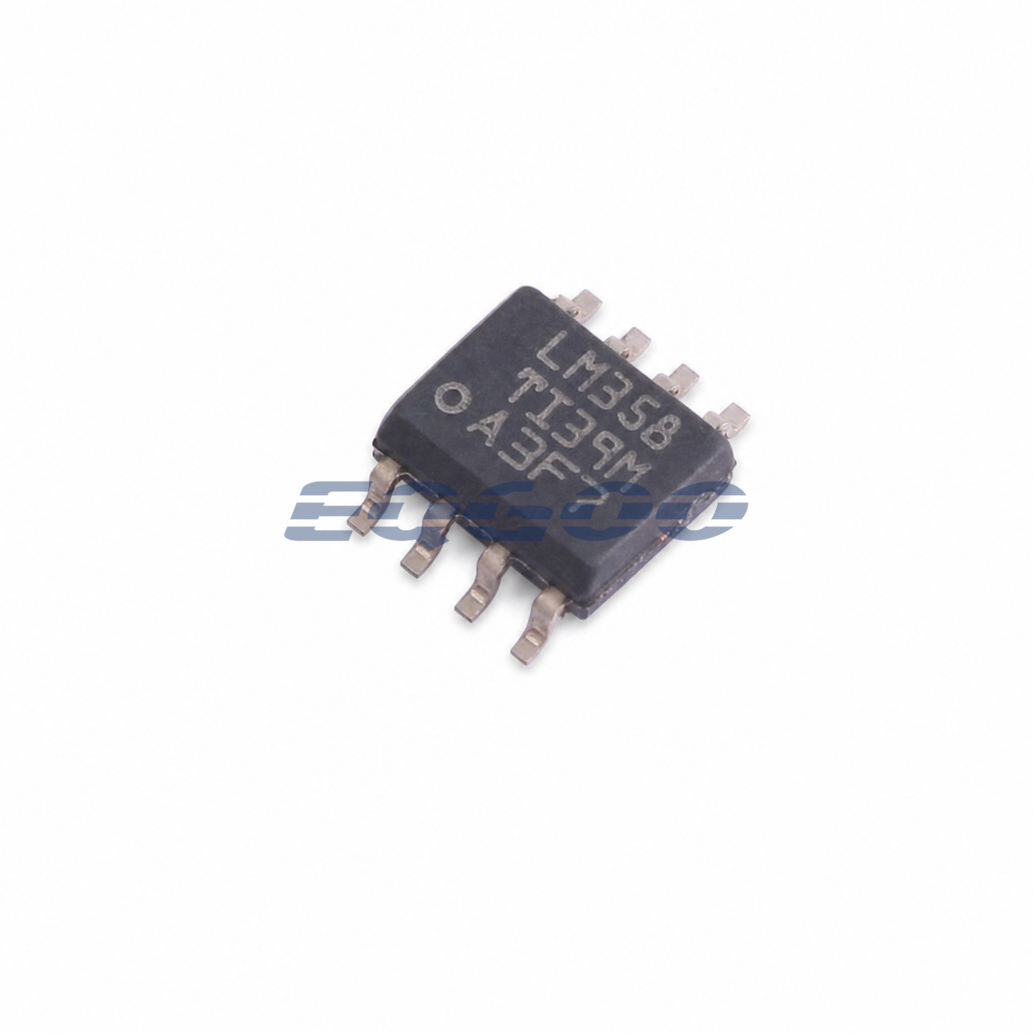
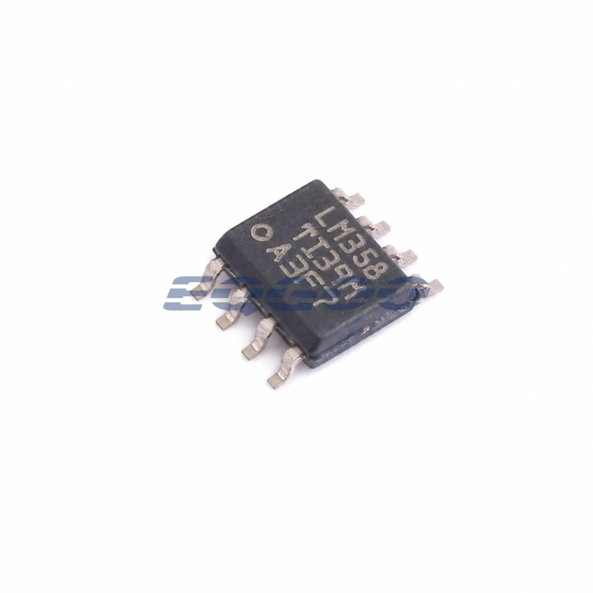

Key Selection Information
| Selection Parameter | Confirmed Information |
|---|---|
| Manufacturer | Texas Instruments |
| Manufacturer Part Number | LM358DR |
| Manufacturer Status | ACTIVE |
| Channels | 2 |
| Architecture | Bipolar operational amplifier |
| Total Supply Voltage | 3 V to 30 V |
| Gain-Bandwidth Product | 0.7 MHz typical |
| Slew Rate | 0.3 V/µs typical |
| Input Offset Voltage | 7 mV maximum at 25 °C |
| Input Bias Current | 150 nA maximum in TI parametric data |
| Quiescent Current | 0.35 mA per channel typical |
| Common-Mode Input Range | Includes negative supply; upper headroom about 1.5 V below positive rail at 25 °C |
| Output Low-Side Headroom | About 5 mV typical under TI test conditions |
| Output High-Side Headroom | About 2 V below positive rail typical under TI test conditions |
| Package | SOIC-8 (D) |
| Packing | 2,500 units, large tape and reel |
| Operating Temperature Range | 0 °C to +70 °C |
Product Overview
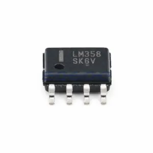
The Texas Instruments LM358DR is the active large-tape-and-reel SOIC-8 ordering code for the classic LM358 dual operational amplifier. It integrates two bipolar op-amp channels and operates from a total supply voltage of 3 V to 30 V, with a typical gain-bandwidth product of 0.7 MHz and a typical slew rate of 0.3 V/µs.
A defining characteristic of the classic LM358 is that its input common-mode range includes the negative supply rail. In a single-supply circuit with V− connected to ground, this allows the amplifier to process input signals near ground without requiring a negative rail. The tradeoff is that the input range does not extend to the positive rail, and the output is also not rail-to-rail on the high side.
The exact LM358DR orderable part is rated for 0 °C to +70 °C operation and supplied in a 2,500-unit large tape-and-reel carrier. TI currently lists the part as ACTIVE.
Key Features
- Two operational-amplifier channels in one SOIC-8 package.
- 3 V to 30 V total operating-supply range.
- 0.7 MHz typical gain-bandwidth product.
- 0.3 V/µs typical slew rate.
- Input common-mode range includes the negative supply rail.
- 7 mV maximum input-offset voltage at 25 °C for the standard LM358 grade.
- 0.35 mA per-channel typical quiescent current.
- Typical low-side output headroom of about 5 mV under TI test conditions.
- 0 °C to +70 °C operating-temperature range for LM358DR.
- Active SOIC-8 large tape-and-reel orderable code.
Technical Specifications
| Group | Parameter | Value |
|---|---|---|
| Amplifier | Channels | 2 |
| Amplifier | Architecture | Bipolar |
| Amplifier | GBW | 0.7 MHz typical |
| Amplifier | Slew rate | 0.3 V/µs typical |
| DC | Input offset voltage | 7 mV maximum at 25 °C |
| DC | Offset drift | 7 µV/°C typical |
| Input | Input bias current | 150 nA maximum in TI parametric data |
| Input | Common-mode low-side headroom | 0 V typical relative to V− |
| Input | Common-mode high-side headroom | About 1.5 V below V+ at 25 °C |
| Output | Typical low-side headroom | About 5 mV |
| Output | Typical high-side headroom | About 2 V below V+ |
| Supply | Total supply voltage | 3 V to 30 V |
| Supply | Quiescent current | 0.35 mA/channel typical |
| Noise | Voltage-noise density at 1 kHz | 40 nV/√Hz typical |
| Package | Type | SOIC-8 (D) |
| Package | Carrier | 2,500-unit large tape and reel |
| Operating | Temperature | 0 °C to +70 °C |
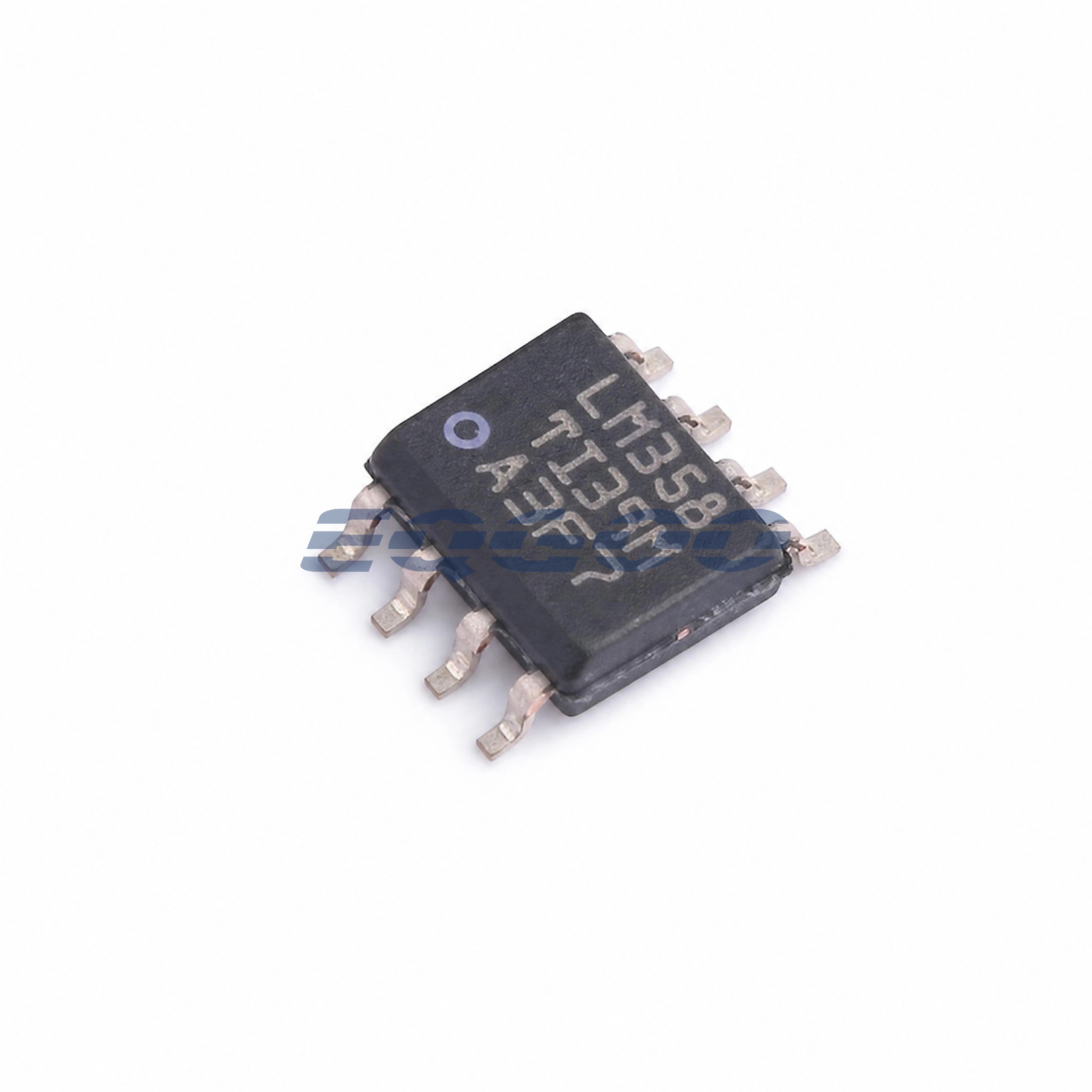
Product Status
| Item | Information |
|---|---|
| Manufacturer Status | ACTIVE |
Texas Instruments currently lists LM358DR as an active production orderable part. TI also lists the tube-carrier LM358D as obsolete, so the carrier suffix matters when evaluating lifecycle for the exact orderable code.
Functional Highlights
Ground-sensing input range on a single supply
With V− connected to ground, the common-mode input range reaches the negative rail. This is useful in signal-conditioning circuits that need to process low-level signals near ground without creating an artificial mid-supply bias solely to keep the input stage inside its common-mode range.
Not rail-to-rail on the positive side
The same input stage that permits ground sensing does not extend to the positive rail. TI specifies the common-mode ceiling about 1.5 V below V+ at 25 °C, and the output also requires significant high-side headroom. Designs that must sense or drive close to the positive rail should use an amplifier whose input/output architecture explicitly supports that requirement.
Moderate bandwidth for general-purpose analog stages
The 0.7 MHz GBW and 0.3 V/µs slew rate place LM358DR in low-to-moderate-speed analog work. It can support DC amplification, low-frequency active filters, buffering, and sensor conditioning when the closed-loop bandwidth and large-signal settling requirements fit these limits.
Offset and bias current set the DC accuracy floor
The standard LM358 grade allows up to 7 mV input offset at 25 °C. In high closed-loop gain or small-signal measurement circuits, that offset can become a significant output error. Input-bias current can also create additional error through source resistance, so precision designs should calculate those terms rather than relying only on nominal gain.
Applications / Application Fit
LM358DR can be considered for general-purpose analog stages where two channels, a 3 V to 30 V supply range, ground-sensing inputs, and moderate bandwidth are sufficient.
Typical engineering fits include:
- low-frequency sensor-signal conditioning;
- buffering and level scaling for ADC inputs that remain inside the LM358 input/output ranges;
- active filters and DC gain stages;
- current- or voltage-monitoring circuits where the sensed input remains inside the common-mode range;
- analog utility functions in commercial-temperature control and interface electronics.
The device is not the first choice for high-speed signal paths, precision instrumentation, rail-to-rail input/output requirements, or operation outside 0 °C to +70 °C. Those cases should use a device with the required bandwidth, offset, temperature grade, or rail-to-rail architecture.
Why Choose This Part
LM358DR makes technical sense when the design needs two low-cost, general-purpose op-amp channels in SOIC-8, operates from a total supply of 3 V to 30 V, and benefits from an input range that includes the negative supply. Its long-established pinout can also simplify maintenance of existing LM358-based designs.
For new designs that need improved performance, TI identifies LM358B as a pin-compatible upgrade family with wider supply capability, higher GBW, lower quiescent current, tighter offset, and a wider operating-temperature range on the applicable ordering codes. That upgrade should be evaluated against the exact application’s requirements rather than treated as automatically interchangeable in every electrical condition.
Design Considerations
Input common-mode range: Ground sensing does not mean rail-to-rail input. At 25 °C the upper common-mode limit is approximately V+ − 1.5 V; over temperature, the guaranteed margin can be larger. Keep the intended input signal inside the datasheet range.
Output swing: The output can approach the negative rail under light-load test conditions but remains roughly 2 V below the positive rail in TI’s typical parametric data. Verify actual output headroom at the intended load current and supply voltage.
Offset error: With up to 7 mV input offset at 25 °C, high-gain DC circuits can accumulate substantial output error. Calculate the maximum closed-loop offset contribution when accuracy matters.
Bias-current error: Source resistance converts input-bias current into additional input-referred error. Use appropriate source impedance or a lower-bias-current amplifier when this term becomes significant.
Bandwidth and slew rate: Closed-loop bandwidth is lower than the 0.7 MHz GBW, and large-signal performance is further limited by the 0.3 V/µs slew rate. Check both small-signal and large-signal requirements.
Absolute maximum input ratings are not operating ranges: TI documents large differential- and single-ended-input stress limits, but those are protection / absolute-maximum constraints. They must not be used as a normal common-mode operating range or as a reason to expose the input deliberately to out-of-range transients.
Temperature grade: LM358DR is specified for 0 °C to +70 °C. Use a different exact ordering code or family when operation outside that range is required.
Related Engineering Resources
- Texas Instruments LM358 product page — official parametric data, datasheet, design resources, and upgrade information.
- Texas Instruments LM358DR part details — exact ordering-code lifecycle, package, carrier, and quality information.
- TI LM324/LM358 design guidelines — manufacturer application guidance for circuits based on the classic LM324/LM358 core.
FAQ
What supply voltage does LM358DR support?
The classic LM358 operates from a total supply voltage of 3 V to 30 V.
Can the inputs sense ground on a single-supply circuit?
Yes. The common-mode input range includes the negative supply, so with V− tied to ground the inputs can operate at ground under the applicable datasheet conditions.
Can the inputs sense the positive rail?
No. The classic LM358 is not rail-to-rail input. The upper common-mode limit is below V+.
What is the maximum input-offset voltage?
TI specifies 7 mV maximum at 25 °C for the standard LM358 grade.
Is LM358DR suitable for precision measurement?
It can be used where the resulting offset, bias-current, noise, bandwidth, and drift errors are acceptable, but it is not a precision op amp. Small-signal high-gain measurement often benefits from a lower-offset and lower-bias-current device.
What does DR mean?
The exact LM358DR part uses the D-package SOIC-8 and a 2,500-unit large tape-and-reel carrier. TI lists this exact orderable code as ACTIVE.
Quality & Verification Support
Third-party inspection or testing can be arranged according to customer requirements. Testing fees are borne by the buyer. Additional verification requirements can be discussed before shipment. After an order is placed, physical product, label, packaging, and Date Code photos may be provided where appropriate.
Request a Quote
To request a quotation, provide the manufacturer part number, required quantity, destination, target Date Code if applicable, and any testing or inspection requirements.