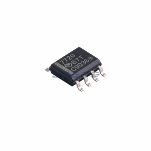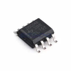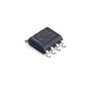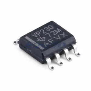
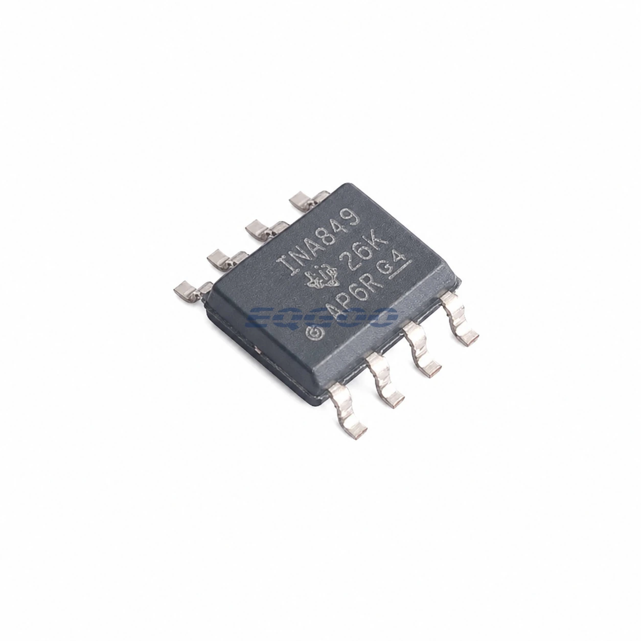

Key Selection Information
| Selection Parameter | Confirmed Information |
|---|---|
| Input Voltage Noise | 1 nV/√Hz typical |
| Offset Voltage | 35 µV maximum |
| Offset Drift | 0.4 µV/°C maximum |
| Bandwidth | 28 MHz at G=1; 8 MHz at G=100 |
| Slew Rate | 35 V/µs |
| Gain Range | 1 V/V to 10,000 V/V |
| Supply | 8 V to 36 V or ±4 V to ±18 V |
| Exact Package / Packing | SOIC (D), 8 pins; 2500-piece large tape and reel |
Product Overview
INA849DR is the high-speed, ultra-low-voltage-noise member of this instrumentation-amplifier set. Its 1 nV/√Hz typical voltage noise, 28 MHz G=1 bandwidth and 35 V/µs slew rate target high-resolution acquisition of fast, very small differential signals.
Unlike micropower sensor amplifiers, INA849 requires an 8 V minimum single supply or ±4 V dual supplies and is selected primarily for signal fidelity rather than battery life. At gain 100 it still provides about 8 MHz bandwidth, which can support direct drive of high-resolution ADC stages when settling and anti-alias filtering are designed correctly.
The current-feedback topology keeps bandwidth high as gain increases. That same speed makes layout, supply bypassing, REF impedance, source impedance and ADC input network more critical than with slower instrumentation amplifiers.
For related devices, see HKEQGOO’s Instrumentation Amplifiers category.
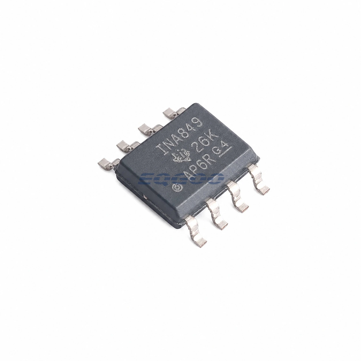
Technical Specifications
| Parameter | Verified Information |
|---|---|
| Manufacturer | Texas Instruments |
| Exact MPN | INA849DR |
| Input Voltage Noise | 1 nV/√Hz typical |
| Offset Voltage | 35 µV maximum |
| Offset Drift | 0.4 µV/°C maximum |
| Bandwidth | 28 MHz at G=1; 8 MHz at G=100 |
| Slew Rate | 35 V/µs |
| Gain Range | 1 V/V to 10,000 V/V |
| Supply | 8 V to 36 V or ±4 V to ±18 V |
| Exact Package / Packing | SOIC (D), 8 pins; 2500-piece large tape and reel |
| Manufacturer Status | Active / Production |
| Part Marking | INA849 |
Functional Highlights
1 nV/√Hz shifts the noise budget toward the sensor and resistor network
In low-source-impedance systems, amplifier voltage noise can be small enough that sensor thermal noise, gain resistor noise and ADC noise become dominant. That benefit is lost if high-value source resistance raises current/Johnson noise.
Fast settling supports high-resolution ADC acquisition
TI cites 0.4 µs settling to 0.01% and multi-MHz bandwidth at high gain. ADC input charge kickback, RC filtering and reference-pin drive should be designed so the amplifier remains stable and settles within the converter acquisition window.
Design Considerations
- Use very short, symmetric input and RG routing; parasitic capacitance matters at tens of MHz.
- Place low-ESR supply bypass capacitors directly at both supply pins.
- Keep REF source impedance low and verify ADC drive/filter stability instead of connecting a high-impedance divider directly.
Product Status and Exact Order Code
Manufacturer status: Active / Production
Texas Instruments lists INA849DR as Active / Production; SOIC (D), 8 pins; 2500-piece large tape and reel; Level-2-260C-1 YEAR; −40°C to +125°C; marking INA849.
Related Engineering Resources
Quality & Verification Support
Third-party inspection or testing can be arranged according to customer requirements. Testing fees are borne by the buyer. Additional verification requirements can be discussed before shipment. After an order is placed, physical product, label, packaging, and Date Code photos may be provided where appropriate.
Request a Quote
To request a quotation, provide the manufacturer part number, required quantity, destination, target Date Code if applicable, and any testing or inspection requirements.