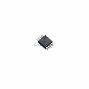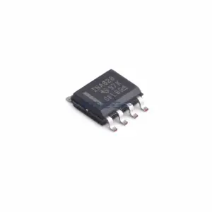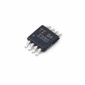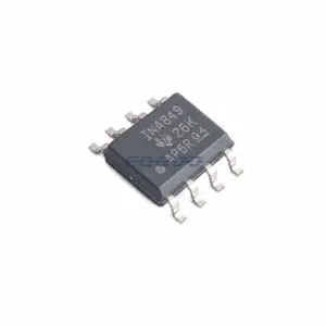

Key Selection Information
| Selection Parameter | Confirmed Information |
|---|---|
| Architecture | Zero-drift precision instrumentation amplifier |
| Supply | 1.8 V to 5.5 V |
| Quiescent Current | 50 µA |
| Gain Range | 1 V/V to 1000 V/V |
| Offset / Drift | 25 µV maximum and 0.1 µV/°C at G ≥ 100 |
| Input Bias | 200 pA maximum |
| Output / Inputs | Rail-to-rail output; RFI-filtered inputs |
| Exact Package / Packing | SON (DRG), 8 pins, 3 mm × 3 mm; 3000-piece large tape and reel |
Product Overview
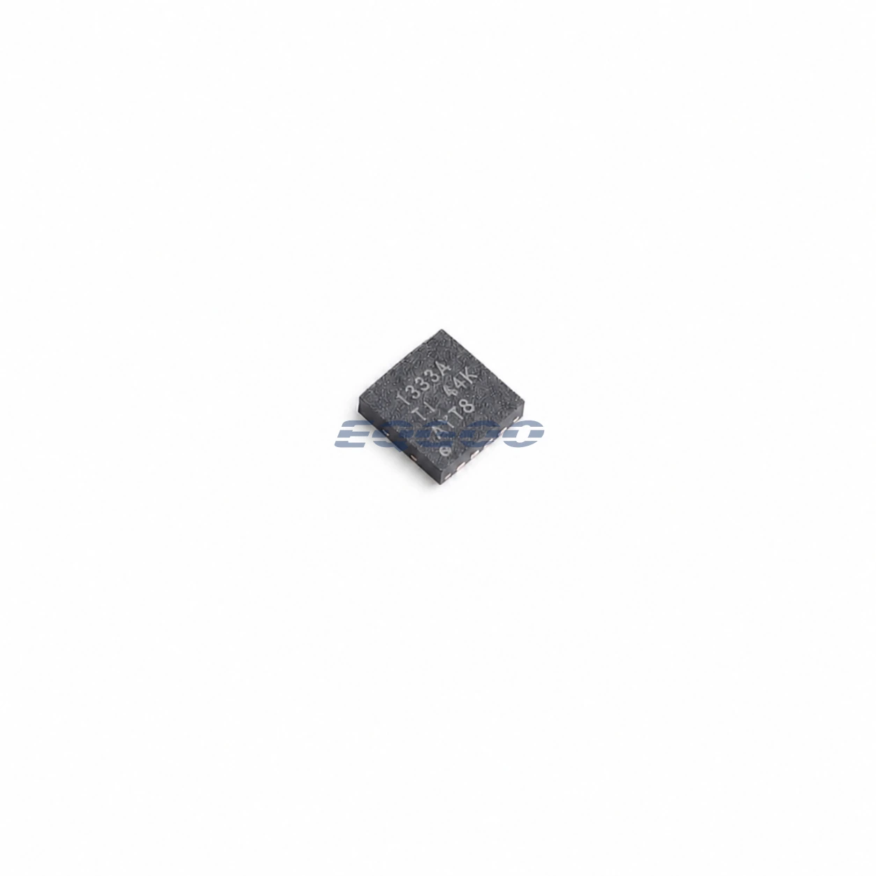
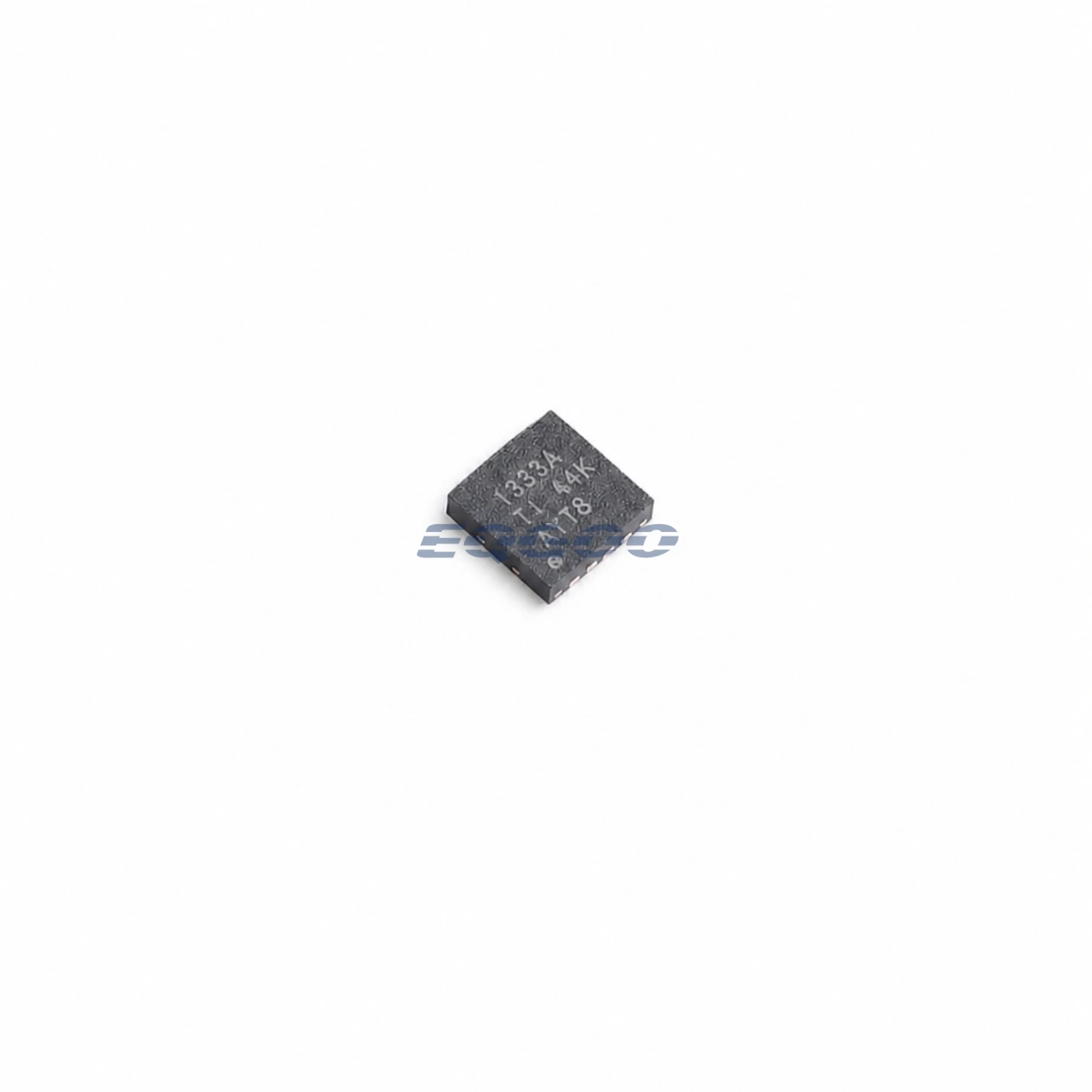
INA333AIDRGR places the low-power zero-drift INA333 core in a 3 mm × 3 mm leadless SON package. The electrical function remains a 1.8 V to 5.5 V, 50 µA instrumentation amplifier with gain from 1 to 1000, but the package choice targets compact, high-density sensor electronics.
A leadless DRG footprint reduces board area and can shorten sensitive analog routing between the sensor, gain resistor and ADC. It also changes assembly and inspection: solder joints are less visually accessible than on DGKR VSSOP, and land pattern, paste deposition and thermal-pad/ground treatment must follow the package drawing.
For battery-powered bridge or biopotential front ends, the main electrical benefit remains zero-drift DC precision at very low supply current. The DRGR order code is chosen when that performance must fit into a tighter PCB area.
For related devices, see HKEQGOO’s Instrumentation Amplifiers category.
Technical Specifications
| Parameter | Verified Information |
|---|---|
| Manufacturer | Texas Instruments |
| Exact MPN | INA333AIDRGR |
| Architecture | Zero-drift precision instrumentation amplifier |
| Supply | 1.8 V to 5.5 V |
| Quiescent Current | 50 µA |
| Gain Range | 1 V/V to 1000 V/V |
| Offset / Drift | 25 µV maximum and 0.1 µV/°C at G ≥ 100 |
| Input Bias | 200 pA maximum |
| Output / Inputs | Rail-to-rail output; RFI-filtered inputs |
| Exact Package / Packing | SON (DRG), 8 pins, 3 mm × 3 mm; 3000-piece large tape and reel |
| Manufacturer Status | Active / Production |
| Part Marking | I333A |
Functional Highlights
Compact package can shorten high-impedance sensitive nodes
Short RG and input traces help reduce parasitic pickup and leakage around a precision sensor front end. Board cleanliness and matched input routing still matter at high gain.
Assembly process becomes more important than with VSSOP
Leadless SON assembly depends more heavily on stencil, pad and reflow control. A package swap from DGKR to DRGR should therefore be treated as a PCB/production change even when the electrical schematic is unchanged.
Design Considerations
- Use the TI DRG land pattern and controlled solder process; do not reuse a VSSOP footprint.
- Keep RG and differential input traces short and symmetric to preserve CMRR.
- Verify thermal/ground pad implementation against the exact package drawing before production.
Product Status and Exact Order Code
Manufacturer status: Active / Production
Texas Instruments lists INA333AIDRGR as Active / Production; SON (DRG), 8 pins, 3 mm × 3 mm; 3000-piece large tape and reel; Level-2-260C-1 YEAR; −40°C to +125°C; marking I333A.
Related Engineering Resources
Quality & Verification Support
Third-party inspection or testing can be arranged according to customer requirements. Testing fees are borne by the buyer. Additional verification requirements can be discussed before shipment. After an order is placed, physical product, label, packaging, and Date Code photos may be provided where appropriate.
Request a Quote
To request a quotation, provide the manufacturer part number, required quantity, destination, target Date Code if applicable, and any testing or inspection requirements.